At first, let us understand how to create the next circuit board manufacturing process. Learn how to set or execute a goal or function. Then, in PCB design, this term refers not only to the category of process data, but also to the manufacturer's capabilities. These data are based on the performance of the manufacturer's equipment and the entire design process.

In the plate making process, the most important three control points: etching, drilling and positioning, other properties will also affect the entire process category.
With the upgrading of craftsmanship, craft categories are also divided into: traditional, advanced, leading and most advanced. The data will continue to be updated, so the rules of the process category will change.
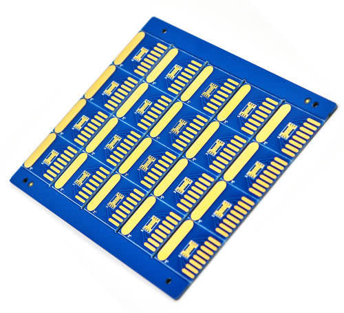
Circuit board technology
Process category and general definition:
Conventional process: The lowest and most common level of this process, usually 0.006 inches is 10.006 inches (6/6 mi), 0.012 inches (0.3048 cm) and 8*10 printed circuit boards (PCB) are limited.
Advanced technology: In the second stage of the process, there is a limit of 5 miles in size and at least 0.008 inches of drilling (0.2032cm), and the maximum number of layers of the printed circuit board is 15*20.
3. Leading craftsmanship: basically the highest manufacturing level commonly used, and its limited size is about 22 miles.
The minimum drilling volume is 0.006 inches (0.1524cm), and the maximum number of layers on the printed circuit board is 25*30.
4. There is no clear definition of the most advanced processes, because the processes at this level often change, their data changes over time and need to be constantly adjusted.
Note: Most common specifications in the industry are based on traditional processes, even if they are based on 0.5 ounces of initial copper foil.

In this process, the following are the key terms and data of timing design, these terms and data are often used in this book and industry
Minimum wire: The minimum wire width is determined by the thickness of the steel. The above table is the most general thickness.
Minimum distance: The increase in copper thickness in the same object. In addition, the minimum distance is determined by data related to it.
Thickness to aperture ratio: a ratio value. The first data is basically the divisor of the second data. For example, 8:1 means that the aperture pitch is 0.008 inches, and the thickness is 0.064 m inches divided by 8. The hole diameter of a thick plate with a thickness of 0.125 is not less than 0.015 inches.
Minimum drilling: The manufacturer has restrictions on the size of the hole, which means the smallest hole that can be used and the smallest hole that can be maintained.
Drilling tolerance: Drilling tool tolerance is one of the factors that determine manufacturing technology. For some reasons, drilling is usually imperfect, and drilling tolerances specify the range of completed holes.
Hole wall (electroplating): After drilling the printed circuit board, put the printed circuit board into the electrolytic tank, make the copper plate fall off, the printed pole is charged, the steel is attracted, and the accessory becomes the cycle of the hole. Set of simple structures.
Copper plating: occurs during the electroplating process of the hole, the phenomenon is that the copper adheres to the copper layer that still has dew. Plating is the basic feature of the hole plating process.
Minimum mask gap: the area surrounded by pads or holes in order to consider the positioning error of the mask.
Mask position: The position of the mask, including the top image, data or hole on the board.
Minimum mask thickness: used to measure the position from the top layer to the screen printing layer.
Screen printing positioning: used to measure the height of screen printing fonts to reach the required height.
Screen printing thickness: The line width of screen printing characters is the stroke width.