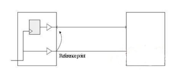
Another special case of the common clock system is the internal synchronous clock system. Many inexperienced engineers will misjudge the internal synchronous clock system as source synchronous timing, and perform equal length control according to the source synchronous timing, resulting in timing design errors.
First of all, let's review how to determine whether a system is a common clock. The previous blog post mentioned that finding a clock tree and determining the relationship between clock signals is the key to judging various timing systems. Common clock system generally has an external crystal or crystal, which is connected to the driving end and receiving end of the system through a clock distributor (or FPGA can directly output different clocks to the driving end and the receiving end), and the external clock line To control the timing of the system, it is called a common clock system.
The clock signal of the internal synchronization clock is sent directly from the driving end to the receiving end. The previous blog post mentioned that the timing margin of the common clock system is small, and one of the key factors that cannot continue to increase the frequency is Tco. Due to factors such as process, it is difficult to make this Tco too small. For example, the Tco max of SDRAM is general. There are 5.4ns. The internal synchronous clock system replaces the external clock driver with an internal Buffer, so that the Buffer on the clock signal and the Buffer on the data signal can be matched to cancel each other, so that the range between the maximum and minimum values of the device's Tco can be reduced and increased Timing margin makes the timing easy to meet.

The internal synchronization clock system is easy to confuse with the source synchronization. In fact, it is easy to distinguish it by grasping a principle. The source synchronization timing generally exists in the system clock and the strobe signal of the data group, such as the relationship between DQ and DQS and CLK. The internal synchronous clock has only one clock signal shared by the driving end and the receiving end (in Mobile SDRAM, the signal name is SDCK)
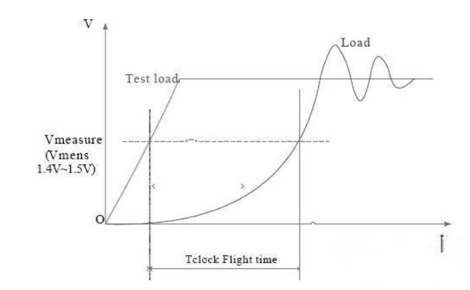
Therefore, the internal synchronization timing is similar in calculation to the common clock, except that there is one more variable in the inequality, which is TCLK_FT: Flight time of Clock. Figure 2 shows the measurement method of TCLK_FT.

The timing calculation formula of the internal synchronization clock is: (when the propagation direction of the clock and the data are the same, it is the positive direction)
Tco(max)+Tflight(max)+Tsetup-Tclk_ft+Tjitter+Tmargin Tco(min)+Tflight(min)-Tclk_ft-Tmargin>Thold In this way, the clock can be in the best position by adjusting Tclk_ft. This method can also be used to adjust the timing in the external synchronization mode. The specific adjustment method has been introduced in the previous case, you can refer to it. Summary: From an external point of view, internal synchronization and source synchronization are the same, but the internal structure of the two is different. The source synchronization method is to add a register before the buffer of the clock signal in the internal synchronization structure, and the clock processing and data processing inside the chip are the same. In this way, the clock can change with the speed of the data and is always in the middle of the data. The essence of the internal synchronization clock is still the common clock system. The timing calculation is the same as the common clock system of the external clock, except that Tclk_ft is added or subtracted at both ends of the calculation result. The timing constraint relationship is also the way of the maximum and minimum total length, not the way of equal length. The internal synchronous clock increases the means of timing margin adjustment, and because it offsets the influence of Tco, the timing is easier to meet. However, the timing calculation method is more complicated and requires the design engineer to grasp it.