An image plane is a layer of copper conductors (or other conductors) that is located inside a printed circuit board (PCB). It may be a voltage plane, or a 0V reference plane adjacent to a circuit or signal routing layer. In the 1990s, the concept of the image plane was widely used, and now it is a proper term for industry standards. This article will explain the definition, principle and design of the image plane.
Definition of image plane
The RF current must return to the current source via a previously defined path or other path; in short, this return path is a kind of image plane. The image plane may be a mirror image of the original wiring (mirror image), or another path located nearby----that is, crosstalk; the image plane may be a power plane, a ground plane, or a free space (free space). space). RF current will be coupled to any transmission line in the form of capacitance or inductance, as long as the impedance of this transmission line is smaller than the impedance of the previously defined path. However, in order to comply with EMC standards, free space must be avoided as a return path.
Although a single-sided PCB can reduce costs, this simple structure may not meet EMC standards. Most 2-layer or 4-layer PCBs have relatively high signal integrity and can pass EMC tests. The high-density (multi-layer board) PCB stack can provide 6dB to 8dB radio frequency suppression for each pair of image planes, which is due to the effect of eliminating magnetic flux. There is a simple rule that can be used to determine when to use a multilayer board: When the frequency rate exceeds 5MHz, or the rise time is faster than 5 ns, a multilayer board must be used.
Definition of inductance
Both traces and copper planes have a limited number of inductances. When a voltage is applied to the traces or transmission lines, these inductances will prohibit current generation, so the two wires become unbalanced common mode radiation, and the magnetic flux cannot be reduced. In the circuit board structure, there are three different types of inductance:
.Partial inductance: the inductance that exists in the wire or PCB trace.
.Self inductance: the inductance from a section of wire, as opposed to an infinitely long section.
.Common partial inductance: the effect of one inductance section on the second inductance section.
Compared with capacitance and resistance, inductance is the most difficult to measure. Inductance represents the dynamic characteristics of a closed current loop. Inductance is the ratio of the magnetic flux passing through a closed loop and the current that produces the magnetic flux. Its mathematical expression is: Lij=Ψij/li, Ψ is the magnetic flux, and I is the current in the loop. In a closed loop, the inductance value is related to the shape and size of the loop. When designing a PCB, engineers often ignore the inductance of the trace. The inductance is always related to the closed loop. The inductance effect of a closed loop can be described by the partial inductance and the common partial inductance effect.
Partial inductance
The internal inductance of a conductor, which is produced by the magnetic flux inside the conductor. The sum of the partial inductances of a closed loop is equal to the sum of the partial inductances of each section, that is,. And the Li of each section is equal to Ψi / li, Ψi represents the magnetic flux coupled to the loop in the i-th section, I is the amount of current in the i-th section, and Li is the partial inductance. Therefore, different circuits will have different values of partial inductance. We are concerned about the partial inductance value, not the total inductance value of the trace. Moreover, the partial inductance can be used to derive the common partial inductance.
Common partial inductance
The main factor that allows the image plane to eliminate magnetic flux is from the "common partial inductance." After the magnetic flux is eliminated, the magnetic lines of force can be connected and the best return path for the radio frequency current can be found. Part of the inductance of itself refers to the inductance of a specific loop section, and has nothing to do with other loop sections. Figure 1 shows a partial inductance of its own. The current in a trace loop is I, and Lp is its own partial inductance of the trace section. Assume that this trace extends from one end of the finite to the other end of infinity.
Theoretically, although part of its own inductance has nothing to do with adjacent wires, in fact, adjacent wires with a small distance will change each other's own partial inductance values. This is because one wire will interact with other wires, so that the current distribution over the entire length of the wire is no longer uniform. Especially when the ratio of the distance between the two wires to the radius is less than 5:1, this situation will be more obvious.
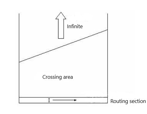
Figure 1: Part of its own inductance
Between the two wires, there will be a common partial inductance. The common partial inductance Mp is based on parallel routing, or the spacing (s) between wire sections. Mp is the ratio of "the magnetic flux generated by the current in the first wire (to a far place through the second wire)" and "the current generated by the first wire". Figure 2 shows a common partial inductance. Its equivalent circuit is shown in Figure 3, and the mathematical expression of this circuit is as follows:
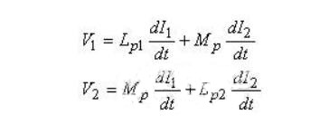
Figure 2: Common partial inductance
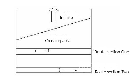
Figure 3: Common partial inductance between two wires
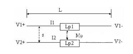
Now with the concept of a common partial inductance, consider transmitting a signal on the circuit of Figure 3, such as a frequency signal. V1 is on the signal path, and V2 is on the RF current return path. Assume that these two wires form a signal path and its return path, so I1 = I and I2 = -I. If it were not for the existence of a common partial inductance, the two wires would not be able to couple with each other, the circuit would not work normally, and would not form a closed loop. The voltage drop in Figure 3 will become:
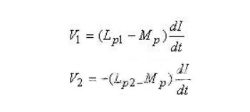
It can be known from the above formula that if the voltage drop is to be reduced, the common part of the inductance (Mp) must be increased.
The easiest way to increase the common part of the inductance is to make the path of the RF return current as close as possible to the signal trace. The best design method is to use a radio frequency return plane near the signal trace. The distance between them should be as small as possible within the achievable range.
Part of the inductance always exists in the wire, it is the same as the default value. Therefore, it is equivalent to an antenna with a specific resonant frequency. "Common partial inductance" can reduce the effect of "partial inductance". By reducing the distance between the two wires, the inductance of individual parts can be reduced, which can meet the requirements of EMI compatibility standards.
In order to maximize the effect of the common part of the inductance, the currents in the two wires must be the same in magnitude, but in opposite directions. This is why the image plane (or ground wire) can be so effective. Between two parallel wires, there are some common inductances, and these inductance values will vary with the distance and length of the two wires (refer to the technical specifications of the wires). When the distance and length of the two parallel wires are the smallest, the inductance value of their common part will be the largest.
If a dielectric material is used to separate the power and ground planes, what role will the "common partial inductance" play at this time? Similarly, as long as the distance between the two planes is small, the inductance value of the common part will be large. At this time, the RF signal current measured on the power plane should be zero.
Because it is offset by the RF return current of the same size and opposite direction.
In addition, it should be noted that if the inductance value of the common part between the two wires is reduced, not only the effect of the image plane will be reduced, but the capacitance value between the two planes will increase.