An image plane is a layer of copper conductors (or other conductors) that is located inside a printed circuit board (PCB). It may be a voltage plane, or a 0V reference plane adjacent to a circuit or signal routing layer. In the 1990s, the concept of the image plane was widely used, and now it is a proper term for industry standards. This article will explain the definition, principle and design of the image plane.
The design of the image plane
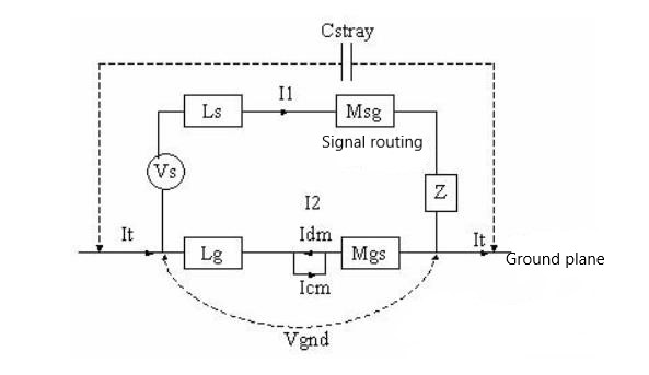
Figure 4 is the image plane in the PCB, which has a common partial inductance. In this figure, most of the RF current of the signal trace will return to the ground plane, which is directly below the signal trace. In this return "image" structure, the RF return current will encounter a finite impedance (inductance). This return current produces a "voltage gradient (slope)" (the rate of change of voltage per unit path length), also known as "ground-noise voltage". Ground noise voltage will cause part of the signal current to pass through discrete capacitors on the ground plane.
The typical common mode current is 1/10n times the differential mode current Idm (n is a positive integer less than 10). However, the common mode current (I1 and Icm) will generate more radiation than the differential mode current (and ). This is because the common mode radio frequency current field is additive, while the differential mode current field is subtractive.
In order to reduce the "ground noise voltage", the common inductance value between the trace and the closest image plane must be increased. This can provide an enhanced path for the return current to map the image current back to the current source. The calculation formula of the ground noise voltage Vgnd is as follows:
Vgnd = Lg dI2/dt-Mgs dI1/dt
Figure 4 and the symbolic meaning of the above formula are as follows:
Ls = part of the inductance of the signal trace itself.
Msg = the common partial inductance between the signal trace and the ground plane.
Lg = part of the inductance of the ground plane itself.
Mgs = the common partial inductance between the ground plane and the signal trace.
Cstray = the stray capacitance of the ground plane.
Vgnd = ground plane noise voltage.
In order to reduce the If in Figure 4, the ground noise voltage must be reduced. The best way is to reduce the distance between the signal trace and the ground plane. In most cases, there is a limit to the reduction of ground noise, because the distance between the signal plane and the image plane cannot be less than a certain value; if it is lower than this value, the fixed impedance and function of the circuit board will not be guaranteed. In addition, it can also provide an additional path for the radio frequency current, thereby reducing the ground noise voltage. This additional return path includes several ground wires.

Figure 4: The ground plane in the PCB
A stable plane will produce common mode radiation. Since the common partial inductance can reduce the generation of radiant radio frequency current, the common partial inductance will also affect the differential mode current and the common mode current. The use of the image plane can greatly reduce these currents. In theory, the differential mode current should be equal to zero, but in fact it cannot be eliminated 100%, and the remaining differential mode current will be converted into a common mode current. This common mode current is the main source of electromagnetic interference. Because the remaining RF current on the return path is added to the main current (I1) in the signal path, causing serious signal interference. In order to reduce the common-mode current, we must increase the inductance value of the common part between the trace plane and the image plane to the maximum in order to capture the magnetic flux, thereby eliminating unnecessary radio frequency energy. Differential mode voltage and current will produce common mode current. In addition to increasing the common inductance value, the method of reducing differential mode current must also minimize the distance between the trace plane and the image plane.
In the PCB, when there is an RF return plane or path, if the return path is connected to a reference source, the best performance can be obtained. For TTL and CMOS, the power and ground pins in the chip are connected to the reference source, power supply, and ground plane. Only when the RF return path is connected to the power and ground pins in the chip, a real image plane will exist. Usually, there is a ground circuit in the chip, and this circuit is connected to the ground plane of the PCB, so a good image plane is produced. If this image plane is removed, an "imaginary" image plane will be created between the trace and the ground plane. Since the distance between the traces is small, the radiated energy will be reduced, so the RF image will be offset. The ideal image plane should be infinite, and there are no splits, crevices or cuts.
Ground and signal return
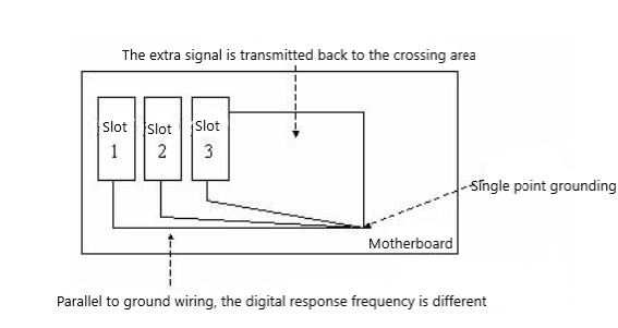
Since the loop is the most important medium for the propagation of radio frequency energy, grounding or signal return loop control (return loop control) is one of the most important design considerations for suppressing electromagnetic interference in the PCB. High-speed logic components and oscillators should be as close as possible to the grounding circuit to avoid forming a loop; there will be eddy currents in this loop, and the chassis or chassis is grounded at this time. Eddy currents are induced by changing magnetic fields and are usually parasitic. Figure 5 shows the loop formed by the PC's adapter card slot and single-point grounding. In this figure, there is an additional signal return loop area. Each loop will produce a different electromagnetic field and frequency spectrum. The radio frequency current will generate an electromagnetic radiation field at a specific frequency, and the size of its radiated energy is related to the area of the loop. At this time, a containment must be used to prevent radio frequency current from coupling to other circuits; or radiation to the external environment, causing electromagnetic interference. However, it is best to avoid RF loop current generated by the internal circuit as much as possible.

Figure 5: Ground loop in the PCB
If the return path of the radio frequency current does not exist, at this time, the ground line connected to the base or the 0V reference source can be used to assist the movement.
Remove bad radio frequency current. This is also called "loop area control".
Control of loop area
A loop induced by a magnetic field, its electromagnetic field can be represented by a voltage source. The size of this voltage source is proportional to the total area of the loop. Therefore, in order to reduce the coupling effect of the magnetic field, the area of the loop must be reduced. The electric field "pickup" receiving system also relies on the loop area to form a receiving antenna.
When there is an electric field, a current source is generated between the power supply and the ground plane. The electric field will not couple from line to line, but will couple from trace to ground, which includes common mode currents. However, for the magnetic field, since the electric field will be generated with it, the electromagnetic field will be coupled from the line to the line, and also from the trace to the ground line.
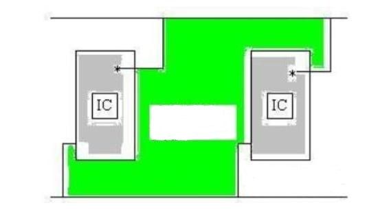
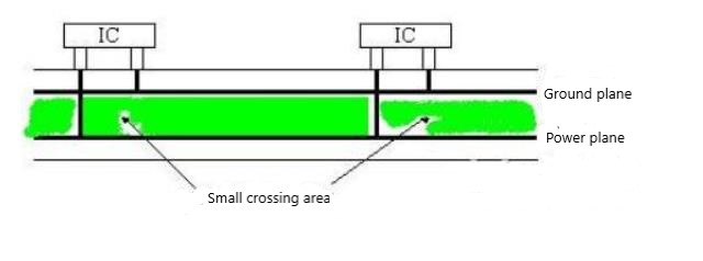
Most people will ignore the need to set a loop area between the power supply and the 0V reference point in the PCB. The large loop area shown in Figure 6 is the easiest to design, but it is also the easiest to be induced by "electrostatic discharge (ESD)" or other fields to become an antenna. Multi-layer stacked PCB can reduce the damage of ESD, and can reduce the generation of magnetic field and prevent it from radiating to free space. In Figure 7, there is a small loop area between the ground plane and the power plane.
Using power and ground planes can reduce the inductance of the power distribution system. If the characteristic impedance of the power distribution system is reduced, the voltage drop of the circuit board can be reduced. If the voltage drop becomes smaller, the phenomenon of "ground bounce" can be avoided. When the logic gate switch is switched quickly, the instantaneous current change will be transmitted to the power plane or ground plane of the motherboard through the IC pins, causing fluctuations in the input reference voltage, and then generating radio frequency noise (RF noise) and electromagnetic interference. The phenomenon is called "ground bounce". In addition, while reducing the characteristic impedance, the capacitance value between the power plane and the ground plane will increase. This capacitance value will make any induced voltage drop. This is the effect of "decouple".

Figure 6: The green area is a large loop area
When the signal line shuttles between the components, a large loop area is created. But we often forget the influence of signal lines on EMI. Although the signal integrity (time domain) is still high, EMI still exists (frequency domain), because the signal loop area causes more problems than power distribution systems. This is especially true from the perspective of ESD; this is because ESD directly enters the input pins of the loop and components. In order to reduce the damage that ESD may cause, reducing the loop area is the easiest way. The power and ground plane decentralized network provides a low-impedance path that can transmit ESD energy to the 0V return reference plane. After all, circuits are circuits, and if they can emit electromagnetic waves, they should be able to receive electromagnetic waves.
In addition to reducing the ground noise voltage, the image plane can also prevent the RF ground loop from becoming larger, because the RF current is tightly coupled with their current source traces, so it does not need to find another return path. When the loop control is maximized, the magnetic flux is greatly eliminated. This is one of the most important concepts for suppressing radio frequency current in PCB. In the vicinity of each signal plane, the correct configuration of the image plane can eliminate the common mode radio frequency current. The image plane that transmits a large amount of radio frequency current must be grounded or connected to a 0V reference point. In order to remove excess RF voltage and eddy currents, all grounding and base planes can be connected to the grounding point of the base through a low-impedance grounding circuit.

Figure 7: PCB layout with a small loop area
Grounding wire spacing
To reduce the loop generation in the PCB, the easiest way is to design many grounding wires, and all of them are connected to the grounding point of the base. Since the edge rate of the component's output signal has been accelerated, multi-point grounding has become a necessary specification, especially when there is a design that uses I/O interconnection. When the PCB uses multi-point grounding, and they are all connected to a metal structure, at this time, we must know the spacing between all grounding wires.
The distance between the ground wires cannot exceed λ/20 of the highest frequency, which includes not only the main frequency but also the harmonic frequencies. If the edge rate of the output signal of a component is relatively slow, the number of grounding points connected to the base can be reduced, or the distance from the grounding position can be increased. For example, the λ/20 of a 64MHz oscillator is 23.4 cm. If the linear distance between the two ground wires is greater than 23.4 cm, there is a possibility that there will be a radio frequency loop, which may be the source of radio frequency energy propagation.
The layout of the components in the PCB must be correct. Putting the ground wires of different functional blocks closely adjacent to each other can shorten the length of the signal trace, reduce reflection, and make it easier to wire, while maintaining the integrity of the signal. The use of vias should be avoided as much as possible, because each via will increase the inductance of the trace by approximately 1 to 3 nH.
In addition, in order to prevent the coupling of different bandwidth areas, different functional blocks must be properly partitioned. The methods include: using separate PCBs, insulation, different wiring... etc. The correct division can improve circuit performance, make winding easier, shorten the length of the trace, and can reduce the area of the loop and improve the signal quality. Before wiring, engineers must plan which components belong to which functional block, and this information can be obtained from component suppliers.