According to a predetermined design, a conductive pattern formed by a PCB board, a printed element or a combination of both is called a PCB board. The fabrication process of the PCB board is introduced below.
Single-sided hard printed board: single-sided copper plate punching (brushing, drying) drilling or perforating anti-corrosion pattern of silk screen line or using dry film curing to repair board anti-corrosion printing material, dry brush cleaning, dry screen printing resistance welding pattern (commonly used Green oil), UV curing screen printing character marking pattern, UV curing screen printing preheating, punching and shape electrical opening, short circuit test cleaning, short circuit test, cleaning, dry pre-coating, oxidation resistance (drying) or tin fog hot air finishing Ping inspection packaging finished product factory.

Double-sided rigid printed boards: double-sided copper laminate CNC drilling through-hole inspection, deburring brush plating (through hole metallization) (full-board electroplating of thin copper) inspection brush cleaning screen printed negative circuit patterns, curing (anti- Nickel etching/gold) inspection, negative circuit pattern inspection, curing (anti-nickel/gold), negative circuit pattern inspection, negative circuit pattern inspection by brush screen printing, negative circuit pattern inspection, curing inspection (nickel resist/ Gold), tin-plated line pattern, tin-plated electroplating (tin removal) printing materials (photosensitive dry film or wet film, exposure, development, thermal curing, commonly used photosensitive thermal curing green oil), usually used for cleaning and brushing screen printing resistance welding patterns Thermal curing green oil (photosensitive anti-corrosion nickel/gold, thermal curing commonly used photoperiod thermal curing green oil) cleaning, drying screen printing marking character patterns, curing (tin spraying or organic welding film) shape processing cleaning, drying electric flux inspection Packaging finished product factory.
Through-hole metallization process of multi-layer boards: double-sided openings and brushing, drilling, light-resistant dry film or photoresist exposure of the inner copper plate, lithography, inner roughening, and roughening of the inner layer of the deoxidized layer (outer layer Single-sided copper clad laminate circuit fabrication, B-stage bonding sheet, board bonding sheet inspection, drilling positioning holes). ), (hot air leveling or organic solder mask)). By brushing the positioning holes, the process of through-hole metallization to manufacture multi-layer laminates is realized. Drilling positioning holes, numerical control drilling pre-processing and electroless copper plating full-plate thin copper coating, photo-resistant electroplating dry film or coating photo-resistant electroplating agent surface layer exposure and development of the bottom plate, chemical copper full-plate thin copper coating inspection and positioning The number of holes is controlled. The light exposure resistance of the electroless copper plating and the light exposure resistance of the thin copper plating on the whole plate is controlled by the number of holes. The development of electroplating dry film or the plating is light to the surface exposure, repairing the line type electroplating tin-lead alloy or nickel/gold plating to remove the etching inspection screen printing Resistance welding pattern or photosensitive welding pattern printing characteristic map (hot air leveling or organic welding film)/NC cleaning shape cleaning, dry electric switch inspection/inspection finished product inspection packaging factory.

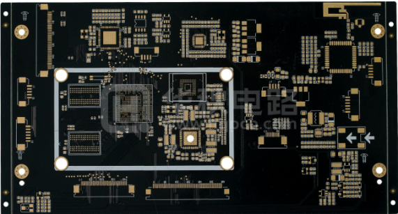
The multilayer PCB board process is developed on the basis of the double-sided metallization process. According to experts from the China Epoxy Resin Industry Association, this process has several unique contents in addition to the double-sided process: inner-layer interconnection of metallized holes, drilling and decontamination, positioning systems, layering, and special materials. Our commonly used computer cards are basically double-sided PCB board boards based on epoxy glass cloth, one of which is plug-in components, and the other side is the soldering surface of the component feet. We can see that the solder joints are very regular. We call the discrete welding surface a solder joint.
Why other copper wires are not tin. Because in addition to the pads and other components, there is a layer of wave-proof welding resistance film on the surface of other components. The surface resistance welding film is mostly green, and a few use yellow, black, blue, etc. Therefore, resistance welding oil is often called green oil in the PCB industry. Its function is to prevent bridging in wave soldering, improve soldering quality, and save solder. It is also a permanent protective layer for PCB board boards to prevent moisture, corrosion, mildew and mechanical scratches. From the appearance point of view, the surface is a smooth and bright green resistance welding film, which is a green oil that is thermally cured for the sheet material. Not only the appearance is good, but also the precision of the solder joints is high, which improves the reliability of the solder joints.
Introduction to PCB fabrication process and reliability design
The ground wire is designed in electronic equipment, and grounding is an important method to control interference. If grounding and shielding can be properly combined, most of the interference problems can be solved. The ground structure of electronic equipment is system, shell (shield ground), digital (logical ground), analog and so on. The following points should be noted in the design of the ground wire:
Correctly choose single-point grounding and multi-point grounding in low-frequency circuits. The signal operating frequency is less than 1 MHz. The wiring and the inductance between the devices have little effect, but the loop formed by the ground loop has a greater impact on interference, and a small amount of grounding should be used. When the signal operating frequency is greater than 10 MHz, the ground impedance becomes larger. At this time, the ground wire impedance should be reduced as much as possible, and the nearest multi-point grounding should be used. When the operating frequency is 1~10 MHz, when point grounding is adopted, the length of the ground wire should not exceed 1 ≤ 20 of the wavelength, otherwise the multi-point grounding method should be adopted.
2. The digital circuit and the analog circuit are separated from the analog circuit board. There are both high-speed logic circuits and linear circuits on the circuit board, so they should be separated as much as possible, and the ground wires of the two should not be mixed and connected to the ground of the power supply terminal. on-line. The grounding area of the linear circuit should be increased as much as possible.
3. If the ground wire is as thin as possible, the ground potential changes with current changes, resulting in unstable timing signal levels of electronic equipment and deterioration of noise resistance. Therefore, the ground wire should be as thick as possible to pass the three allowable currents on the PCB board board. If possible, the width of the ground wire should be greater than 3mm.
4. The ground wire forms a closed loop. When designing a PCB board board ground wire system consisting only of digital circuits, turning the ground wire into a closed loop can significantly improve the anti-noise ability of the ground wire. The reason is that there are many integrated circuit components on the PCB board board, especially when there are many power consumption components, due to the limitation of the thickness of the grounding line, a large potential difference will appear at the grounding terminal, resulting in a decrease in noise resistance. If the grounding structure is turned into a loop, the potential difference will be reduced and the anti-noise capability of electronic equipment will be improved.