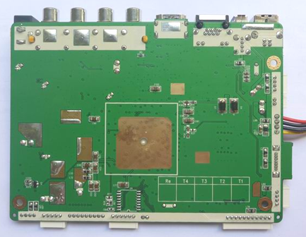
With the continuous improvement of human requirements for the living environment, the environmental issues involved in the PCBproduction process have received more and more attention.
Why do we need special treatment on the PCB surface?
The most basic purpose of PCB surface treatment is to ensure good solderability or electrical properties. Because the copper in the air is easy to oxidize, the copper oxide layer has a great influence on welding, and it is easy to form false welding, which will seriously cause the pads and components to be unable to be welded. Therefore, a process will appear in the production and manufacturing of PCBs, that is, the lining The surface of the pad is coated (plated) with a layer of material to protect the pad from oxidation.
1. Lead-Free PCB
At present, the PCB instant noodle processing technology of domestic board factories includes: spray tin (HASL, hotairsolderleveling), hot solder leveling, hot air leveling, OSP (anti-oxidation), nickel-gold plating, tin precipitation, silver deposition, chemical nickel-palladium-gold, electroplating Hard gold, etc. Of course, there will be some special PCB surface treatment processes in special applications.

2. Spray tin (hot air leveling)PCB
The general process of hot air leveling is: micro-corrosion, preheating, tinning, spray washing.
Hot-air straightening, also known as hot-air soldering (commonly known as tin spraying), is to coat molten tin (lead) solder on the surface of the PCB and heat compressed air to straighten it to form a layer of copper oxidation resistance and good solderability. Floor. The solder and copper form a copper-tin intermetallic compound at the junction of the hot air conditioning solder and copper. PCB is usually immersed in molten solder for hot air finishing; the air knife flattens the liquid solder before the solder solidifies; the air knife minimizes the shape of the meniscus of the solder on the copper surface and prevents solder bridging.
Hot air is divided into vertical type and horizontal type. It is generally considered that horizontal type is better, mainly because the horizontal hot air leveling coating is more uniform and can realize automatic production.
Advantages: low price, good welding performance.
Disadvantages: Due to the poor surface finish of the spray tin plate, it is not suitable for welding thin gap pins and too small parts. Solder beads are prone to produce solder beads during PCB processing, and are prone to short-circuit to fine pitch components. When used in the double-sided SMT process, because the second surface has been reflowed at high temperature, the TiN spray remelting is likely to produce tin beads or similar water droplets into the spherical tin spots affected by gravity, resulting in uneven surface, thus affecting Welding problem.
2. Organic Solderability Preservative (OSP)PCB
The general process is as follows: degreasing->; micro-corrosion>; pickling>; pure water cleaning>; organic coating>; cleaning, process control is easier than other processes, indicating that the treatment process is easier.
OSP is a process for surface treatment of printed circuit board (PCB) copper foil according to the RoHS directive. It is estimated that about 25% of PCBs currently use the OSP process, and the OSP process has been on the rise (it is likely that the OSP process has now surpassed tin spraying and ranks first). OSP process can be used for low-tech PCB or high-tech PCB, such as single-sided TV and PCB, high-density chip packaging board, etc. For BGA, there are also many OSP applications. If the PCB does not have the functional requirements for surface connection or storage time limitation, the OSP process will be the most ideal surface treatment process.
Advantages: simple process, smooth surface, suitable for lead-free soldering and SMT. Convenient rework, convenient production and operation, suitable for horizontal operation. It is suitable for coexistence of various processes (such as OSP+ENIG), low cost and environmentally friendly.
Disadvantages: The number of reflow soldering is limited (the film will be damaged if the thickness of multiple soldering is repeated, and there is basically no problem with 2 times). Not suitable for crimping technology and wire binding. Visual inspection and electrical measurement are not convenient. SMT needs nitrogen protection. SMT rework is not applicable. Need higher storage conditions.
3. The whole board is nickel-plated goldPCB
Gold-plated PCB surface is coated with a layer of nickel and then with a layer of gold. Nickel plating is mainly to prevent the diffusion between gold and copper. There are two kinds of nickel plating: soft gold (pure gold, the gold surface does not look bright) and hard gold plating (the surface is smooth and hard, wear-resistant, contains cobalt and other elements, and the gold surface looks brighter). Soft gold is mainly used for the gold wire of chip packaging, and hard gold is mainly used for electrical connection of non-welded parts.
Advantages: long storage time>; 12 months. Suitable for contact switch design and gold wire wrapping. Suitable for electrical testing.
Disadvantages: high cost and thick gold. When plating gold fingers, additional design lines are needed to conduct electricity. Since the thickness of the gold plating does not necessarily cause the embrittlement of the solder joint, this will affect the strength of the solder joint. The uniformity of the plating surface. The electroplated nickel gold will not wrap the edges of the wire. Not suitable for bundling of aluminum wires.
4. Immersion goldPCB
The general process is as follows: in addition to pickling cleaning>; micro-corrosion>; prepreg->; activation->; electroless nickel plating>; chemical immersion gold; there are 6 chemical baths in the process, involving nearly 100 kinds of chemicals, the process is more complex.
Gold is a thick layer of nickel-gold alloy coated on the copper surface, which can protect the PCB for a long time. In addition, it also has environmental tolerance that other surface treatment processes do not have. In addition, gold can also prevent the dissolution of copper, which will facilitate lead-free assembly.
Advantages: not easy to oxidize, long storage time, smooth surface, suitable for welding fine gap pins and small solder joint components. A key PCB board is preferred (such as a mobile phone board). Reflow soldering can be repeated many times, and the solderability is not significantly reduced. It can be used as the base material of COB (ChipOnBoard) welding wire.
Disadvantages: high cost, poor welding strength, because the electroless nickel process is used, it is prone to black disk problems. The nickel layer will oxidize over time, and long-term reliability is a problem.
5. Sinking tinPCB
Currently, all solders are based on tin, so the tin layer can be matched with any type of solder. The TiN deposition process can form a flat copper-tin intermetallic compound, so that the tin plating layer has the same solderability as the hot air leveling, rather than the hot air leveling; the tin plate cannot be stored for too long and must be assembled in the order of depositing tin.
Advantages: suitable for horizontal production. Suitable for fine wire processing, suitable for lead-free soldering, especially suitable for blanking process. Very good smoothness, suitable for SMT.
Disadvantages: Good storage conditions (preferably no more than 6 months) are required to control the growth of tin whiskers. Not suitable for contact switch design. In the production process, the process requirements of resistance welding film are very high, otherwise the resistance welding film will fall off. It is best to protect nitrogen gas during multiple welding. Electrical testing is also a problem.
6. Immersion SilverPCB
The silver plating process is between organic silver plating and chemical nickel/gold plating, and the process is simple and fast. Even if exposed to heat, humidity, and pollution, silver can still maintain good solderability, but it will lose its luster. Silver does not have the good physical strength of electroless nickel/gold plating because there is no nickel under the silver plating layer.
Advantages: simple process, suitable for lead-free soldering, smooth surface, low cost, suitable for very thin wires.
Disadvantages: high storage conditions and easy contamination. Welding strength is prone to problems (microcavity problem). The copper under the resistance welding film is prone to electromigration and Javanni biting. Electrical measurement is also a problem.
7. Chemical nickel palladium goldPCB
Compared with precipitated gold, chemical nickel, palladium and gold have an extra layer of palladium between nickel and gold. Palladium can prevent corrosion caused by displacement reaction and make adequate preparations for gold deposition. On the other hand, gold is tightly covered by palladium, providing a good contact surface.
Advantages: suitable for lead-free soldering. The surface is very flat and suitable for SMT. The hole can also be coated with nickel and gold. In the long term, storage conditions are not harsh. Suitable for electrical testing. Suitable for switch contact design. Suitable for aluminum wire binding, suitable for thick plates, strong resistance to environmental attacks.
8. Plating hard goldPCB
In order to improve the wear resistance of the product, increase the number of insertion and removal, and electroplate the hard gold.
The surface treatment process of the printed circuit board has not changed much, and it still seems to be a distant matter, but it should be noted that long-term slow changes will lead to great changes. With the increase in environmental protection, the surface treatment process of PCB will surely undergo tremendous changes in the future.