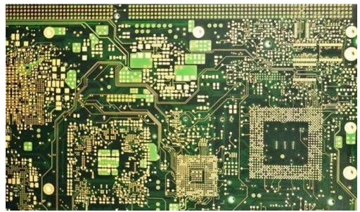
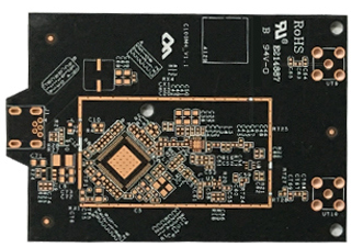
The rapid development of industry is both an opportunity and a challenge for the electronics industry. The PCB blank board of the PCBAfactory passes through the last piece of SMT, and then goes through the whole process of dipping, referred to as PCBA. This is a writing method commonly used in our country. Nowadays, electronic products show the characteristics of miniaturization, light weight and multi-function, and more stringent requirements are put forward on circuit boards. In order to achieve these miniaturization and high integration, it is necessary to use SMT patch processing technology to achieve.
iPCB Circuits Limited is a first-class manufacturer integrating high-precise circuit board and SMT chip processing. In PCB circuit board proofing and SMT patch processing, advanced production equipment, rich production experience and standardized production line can be used for difficult SMT patch processing, special SMT patch processing, SMT Process quick proofing, etc. It can not only meet the complex industrial requirements, but also speed up the production of equipment and provide customers with the best quality and quick service. The following is a detailed understanding of Lepeng Technology's SMT chip processing technology.

1. Programming and placement machine:
According to the template BOM placement map provided by the customer, program the position coordinates of the placement elements, and then use the SMT patch provided by the customer to process the first piece.
2. Printing solder paste:
The solder paste steel is screen printed on the SMD board and needs to be soldered to the pads of the electronic component printer to prepare for component soldering. Before the appearance of printed circuit boards (printing machines), the interconnection of electronic components in the placement plant of printing machine A was based on direct connection of lines, forming a complete line. At present, the circuit board only exists as an effective experimental tool, and the printed circuit board has become an absolute dominant position in the electronics industry. The equipment (printing machine) used is a screen printing machine (printing machine) located at the front end of the SMT patch processing line. Lapeng technology uses KAG automatic printing machine and international brand Lepeng technology solder paste, which not only improves production efficiency, but also ensures welding quality.
3. Patch:
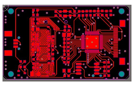
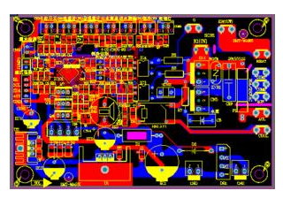
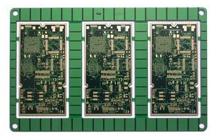
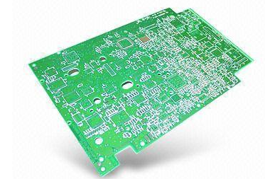
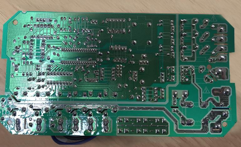
It is to accurately mount the electronic component SMD to the fixed position of the PCB. The printed circuit board manufacturer is a printed circuit board, also known as a printed circuit board, which is an important electronic component, a support for the electronic component, and a carrier for the electrical connection of the electronic component. Because it is manufactured by electronic printing, it is called a "printed" circuit board. The equipment used is a placement machine, located on the back of the SMT production line screen printer. The placement machine used by Lapeng technology is mydata-MY200 high-speed placement machine made in Sweden. This equipment has its own air compressor and does not require an external air compressor. It can stack up to 10 0201 materials and has a high installation accuracy. It is currently one of the most accurate installation equipment in all assembly machine systems.
4. Reflow soldering:
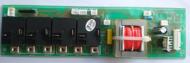
Its main purpose is to melt the solder paste at a high temperature, and then firmly solder the electronic component SMD and PCB board together after cooling. The equipment used is a reflow soldering furnace located at the back of the surfacing machine on the SMTProduce Produce line. Luopeng technology uses Flexonic 10 temperature zone reflow welder with three cooling zones and water towers for cooling. Unlike U-shaped reflow soldering heating tubes of other companies, Lepeng reflow soldering is a sandwich Company with two layers on the heating plate, which makes the heating more balanced.
5. Clean:
The role (role) is to remove harmful solder residues such as flux on the assembled PCB. The equipment used is a washing machine, the location cannot be fixed, it can be online or not online.
6. Test/Check
Mass inspection of PCBAboard welding after welding generally includes the following aspects: surface mount or through-hole insertion, single-sided or double-sided, number of components (including dense feet), solder joints, electrical and appearance characteristics, and key points It is the detection and inspection of the number of components and solder joints. Luopeng Technology uses Ari-off line AOI detectors, X-ray detectors, LCR bridge detectors, 60 times digital electron microscopes and other high-precision test equipment to ensure that the Mass of each product meets the standard.
7. Packing:
Qualified products will be tested and packaged separately. The generally used packaging materials are anti-static foam bags, static cotton, and plastic trays. There are two main packaging methods. One is to use anti-static bubble bags or static cotton to make coils and separate packaging, which is the most commonly used packaging method; the other is to make blister boards according to the size of PCBA. Place it in a plastic tray and unpack it, which is mainly sensitive to needles and contains vulnerable PCBAcomponents.