Abstract: This article discusses the key factors affecting audio characteristics in cellular phone PCB design. A problematic cell phone PCB design and a good PCB layout plan are given in the article. The comparison of the two layouts emphasizes the design considerations for improving audio performance.
Introduction
Cellular phones are the ultimate challenge faced by PCB layout engineers. Modern cellular phones include almost all portable sub-systems, and each sub-system has conflicting requirements. A perfectly designed PCB must give full play to the performance advantages of each interconnected device while avoiding mutual interference between subsystems. Therefore, the performance of each subsystem has to be compromised for conflicting requirements. Although the audio capabilities of cellular phones continue to increase, little attention has been paid to the PCB layout of audio circuits.
Component layout
The first step in any PCB design is of course to choose the PCB placement of each component. We call this step "planning consideration". Careful component layout can reduce signal interconnection, ground wire segmentation, noise coupling, and take up the area of the circuit board.
Cellular phones contain digital circuits and analog circuits. In order to prevent digital noise from interfering with sensitive analog circuits, they must be separated. Dividing the PCB into digital and analog areas helps to improve the layout of such circuits.
Although the RF part of a cellular phone is usually treated as an analog circuit, a common problem that needs to be paid attention to in many designs is RF noise. It is necessary to prevent RF noise from coupling to the audio circuit and generate audible noise after demodulation. In order to solve this problem, it is necessary to separate the RF circuit and the audio circuit as much as possible.
After dividing the PCB into analog, digital, and RF areas, the component layout of the analog part needs to be considered. The component layout should make the audio signal path the shortest, and the audio amplifier should be placed as close as possible to the headphone jack and the speaker, so that the EMI radiation of the class D audio amplifier is minimized, and the coupling noise of the headphone signal is the smallest. The analog audio signal source must be as close as possible to the input end of the audio amplifier to minimize the input coupling noise. All input leads are an antenna for the RF signal, and shortening the lead length helps reduce the antenna radiation effect of the corresponding frequency band.
Component layout example
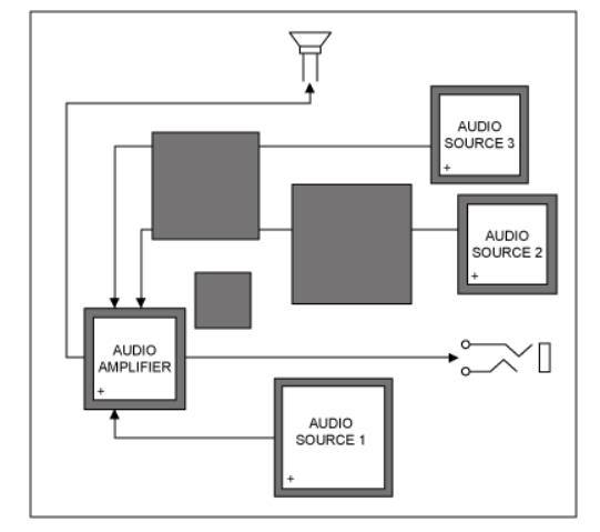
Figure 1 shows an unreasonable audio component layout. The more serious problem is that the audio amplifier is too far away from the audio signal source. The leads pass through the noisy digital circuit and switch circuit, which increases the chance of noise coupling. Longer leads also enhance the RF antenna effect. Cellular phones use GSM technology. These antennas can pick up GSM transmitted signals and feed them into audio amplifiers. Almost all amplifiers can demodulate the 217Hz envelope to a certain extent, producing noise at the output. At worst, the noise may completely submerge the audio signal. Shortening the length of the input lead can effectively reduce the noise coupled to the audio amplifier.
There is another problem with the component layout shown in Figure 1: The op amp is too far away from the speaker and headphone socket. If the audio amplifier uses a class D amplifier, longer headphone leads will increase the amplifier's EMI radiation. This kind of radiation may cause the device to fail the test standards set by the local government. Longer headphone and microphone leads also increase lead impedance and reduce the power that the load can obtain.
Finally, because the components are so scattered, the connections between the components will have to pass through other subsystems. This will not only increase the wiring difficulty of the audio part, but also increase the wiring difficulty of other subsystems.

Figure 1: Unreasonable component layout.
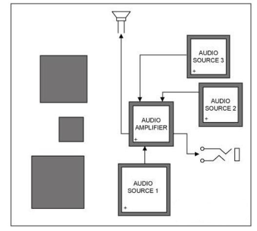
Figure 2 shows the arrangement of the same components in Figure 1. The rearranged components can use space more effectively and shorten the lead length. Note that all audio circuits are distributed near the headphone jack and speakers, the audio input and output leads are much shorter than the above solution, and no audio circuits are placed in other areas of the PCB. Such a design can comprehensively reduce system noise, reduce RF interference, and simple wiring.

Figure 2: A reasonable layout of cellular phones.
Signal pathway
The signal path has a very limited impact on audio output noise and distortion, which means that the compromise measures that need to be provided to ensure performance are very limited.
Speaker amplifiers are usually powered directly by batteries and require considerable current. If you use long and thin power leads, the power ripple will increase. Compared with short and wide leads, long and thin leads have higher impedance, and the current changes generated by lead impedance will be converted into voltage changes and fed into the device. In order to optimize performance, the amplifier power supply should use the shortest possible lead.
Differential signals should be used as much as possible. The differential input has high noise suppression, so that the differential receiver can suppress the common mode noise on the positive and negative signal lines. In order to make full use of the advantages of the differential amplifier, it is very important to keep the same length of the differential signal pair when wiring, so that it has the same impedance, and the two are as close to each other as possible to make the coupling noise the same. The differential input of the amplifier is very effective in suppressing the noise from the digital circuit of the system.
Grounded
For audio circuits, grounding is critical to whether it can meet the performance requirements of the audio system. Unreasonable grounding leads to greater signal distortion, high noise, strong interference, and reduced RF suppression capabilities. It is difficult for designers to invest a lot of time in ground wire layout, but careful ground wire layout can avoid many thorny problems.
There are two important considerations for grounding in any system: first it is the return path of the current flowing through the device, and second it is the reference potential of the digital and analog circuits. It may seem simple to ensure that the voltage at any point of the ground wire is the same, but it is actually impossible. All leads have impedance, and as long as there is current flowing through the ground wire, a corresponding voltage drop will be generated. The circuit leads also form inductance, which means that the current flows from the battery to the load and then back to the battery. There is a certain inductance in the entire current path. When working at higher frequencies, the inductance will increase the ground impedance.
Designing the best ground wire layout for a particular system is not simple. Here are general rules that apply to all systems.
1. Create a continuous ground plane for digital circuits
The digital current of the ground plane returns through the signal path, and the area of the loop should be kept to a minimum to reduce antenna effects and parasitic inductance. Ensure that all digital signal leads have corresponding ground paths. This layer should cover the same area as the digital signal leads, with as few break points as possible. Breakpoints in the ground, including vias, will cause the ground current to flow through a larger loop, thereby generating greater radiation and noise.
2. Guarantee ground galvanic isolation
The ground current of the digital circuit and the analog circuit should be kept isolated to prevent the digital current from interfering with the analog circuit. In order to achieve this goal, the components need to be arranged correctly. If the analog circuit is arranged in one area of the PCB and the digital circuit is arranged in another area, the ground current will be naturally isolated. It is best to have an independent PCB layering for the analog circuit.
3. The analog circuit uses star grounding
Star grounding regards one point of the PCB as a common grounding point, and only this point is regarded as the ground potential. In cellular phones, the battery ground terminal is usually used as a star grounding point. The current flowing into the ground plane will not disappear automatically. All ground currents will flow into this ground point.
The audio amplifier absorbs a considerable amount of current, which will affect the reference ground of the circuit itself and the reference ground of other systems. In order to solve this problem, it is best to provide a dedicated return loop to bridge the power ground of the amplifier and the ground loop of the headphone jack. Note that these dedicated loops do not cross the digital signal line, because they will hinder the digital return current.
4. Maximize the effect of bypass capacitors
Almost all devices require a bypass capacitor to provide transient currents that the power supply cannot provide. These capacitors should be placed as close as possible to the power supply pins to reduce the parasitic inductance between the capacitor and the device pins. Inductance will reduce the effect of the bypass capacitor. In addition, the capacitor must have a low ground impedance, thereby reducing the high-frequency impedance of the capacitor. The grounding pin of the capacitor should be directly connected to the connection layer, and do not pass through a lead to ground.
5. Pour copper on all unused PCB areas as ground layers
When two pieces of copper foil are close to each other, a small coupling capacitance is formed between them. Place a ground wire near the signal wire, and the high-frequency noise on the signal wire will be short-circuited to the ground.
Conclusion
A well-designed PCB is a time-consuming and challenging task, but the investment is indeed worthwhile. A good PCB layout can help reduce system noise, improve RF signal suppression, and reduce signal distortion. A good PCB design will also improve EMI performance and may require less shielding.
If the PCB is unreasonable, there will be problems that could have been avoided during the testing phase. At this time, if measures are taken, it may be too late, and it is difficult to solve the problems faced. It requires more time and effort, and sometimes additional components are added, which increases the cost and complexity of the system.