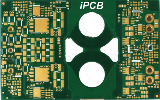
The layout principles of multilayer PCB flexible and multilayer PCB need to follow the following general principles in the circuit board wiring process:
The main contents are as follows:
(1) The principle of setting the distance between printed lines of components. The spacing constraint between different networks is the setting principle of electrical insulation, manufacturing process and spacing between components. Determined by factors such as size. For example, if the pin pitch of the chip is 8M, the [ClearanceConstraint] of the chip cannot be set to 10 million. PCB designers need to set separate PCB design rules for the chip. At the same time, the spacing setting also takes into account the manufacturer's production capacity.
In addition, an important factor affecting components is electrical insulation. If the potential difference between two components or networks is large, electrical insulation needs to be considered. The gap safety voltage in a general environment is 200 V≤mm, which is 5.08V/mil. Therefore, when there are high-voltage circuits and low-voltage circuits on the same circuit board, special attention should be paid to sufficient safety intervals. When there are high-voltage circuits and low-voltage circuits, you need to pay special attention to sufficient safety intervals.

(2) Choice of line type. In order to make the PCB easy to manufacture and beautiful, the corner mode of the wire and the selection of the line type must be set in the PCB design. You can choose 45°, 90° and arc. Generally, sharp angles are not used, and it is best to use arc transition or 45° transition to avoid 90° or sharper corner transitions.
The connection between the wire and the foot pad should also be as smooth as possible to avoid the appearance of small pointed feet, which can be solved by filling in tears. "When the center distance between the pads is less than the outer diameter D of the pad, the width of the wire can be the same as the diameter of the pad; if the center distance between the pads is greater than D, the width of the wire should not be greater than the diameter of the pad. When When the conductor is passed between the two pads but not connected to them, they should be kept at the largest and equal distance; when the wire and the conductor are connected between the two pads and not connected to them, they should be kept at the maximum And equal spacing, the spacing between them should be uniform, equal, and kept to the maximum. The spacing between the two should also be uniform and equal, and should be kept to the maximum.
(3) The method of determining the width of the printing line. The width of the wire is determined by the current level and anti-interference ability of the wire. The larger the current, the wider the wire. The power cable should be wider than the signal cable. In order to ensure the stability of the ground potential, the greater the variation of the ground current, the wider the line should be. Generally speaking, the influence of the power line should be smaller than the width of the signal line, and the ground line should be wider. The experimental results show that when the copper film thickness of the printed conductor is zero. At 05 mm, the current-carrying ground wire of the printing and dyeing line should also be wide, which can be calculated as 20A/mm2, which is 0. 05 mm thick and 1mm wide conductors can flow 1A current. Therefore, the general width can meet the requirements; for high voltage, the width of 10~30 ml can meet the requirements of high voltage, and the signal line width of large current is greater than or equal to 40 ml. The distance between the lines exceeds 30 meters. The large current signal line width is greater than 40 milliliters. The distance between the lines exceeds 30 meters. In order to ensure the stripping strength and working reliability of the wire, the widest possible wire should be used to reduce the line impedance and improve the anti-interference performance within the allowable board area and density.
For the width of the power line and ground line, in order to ensure the stability of the waveform, when allowing the circuit board wiring space, try to thicken it as much as possible, generally at least 50 million.
(4) Anti-interference and electromagnetic shielding of printed wires: Interference on wires mainly includes interference between wires and interference from power lines) Anti-interference and electromagnetic shielding of printed conductors, interference on wires mainly includes interference between wires and Crosstalk between signal lines, reasonable line layout and grounding methods can effectively reduce interference sources, so that PCB design circuit boards have better electromagnetic compatibility.
For high frequency PCB or other important signal lines, such as clock signal lines, it should be as wide as possible on the one hand, and on the other hand, for high-frequency or other important signal lines, such as clock signal lines, it should be as wide as possible. Wire wraps the signal line, which is equivalent to adding a package of ground to isolate it from the surrounding signal lines. It is to "wrap the signal line with a closed ground wire, layer ground shield layer) layer ground shield layer.