Abstract: Faced with the development of electronic products to miniaturization, high density and high speed, the complexity of PCB design has greatly increased. How to effectively control the comprehensive quality of complex PCB design is a topic we are facing. After introducing VALOR's Trilogy 5000 software, the process of applying DFM (manufacturability analysis technology) to the whole process of product PCB design was described, and compared with traditional PCB design and inspection methods. The PCB design review mechanism can assist design, process, manufacturing and quality inspection personnel in the quality control of the product life cycle process. As a powerful tool for automatic review before PCB design is completed to production, it improves the first-time success rate of PCB design. Shorten the product development cycle.
With the rapid development of electronic products, a large number of high-integration devices such as BGA, QFP, PGA and CSP have been used in PCB design. The complexity of PCB has also increased greatly. The subsequent PCB design and manufacture are difficult, and difficult to test. Production problems such as poor soldering, device mismatch and difficult maintenance. This leads to delays in the entire product construction period, longer development cycles, increased costs, high product repair rates, and potential product quality hazards. At the same time, such products cannot meet the requirements of short time, high reliability and high stability of military products.
In the actual design and production process, we introduced the "design for manufacturability" concept through the application of the VALOR software Trilogy 5000 DFM function, and moved the product design quality center forward. Incorporate manufacturing rules in the design phase and establish a new PCB design process, as shown in Figure 1. In order to reduce the cycle extension caused by the design change, the production quality and efficiency are guaranteed. Solve or discover all possible quality hazards in the early stage of manufacturing, minimize the number of iterations of product development, reduce costs, and improve the market competitiveness of products. It also makes product quality irrelevant to the design software used, and has nothing to do with the level of designers, allowing the enterprise to enter standardized management.
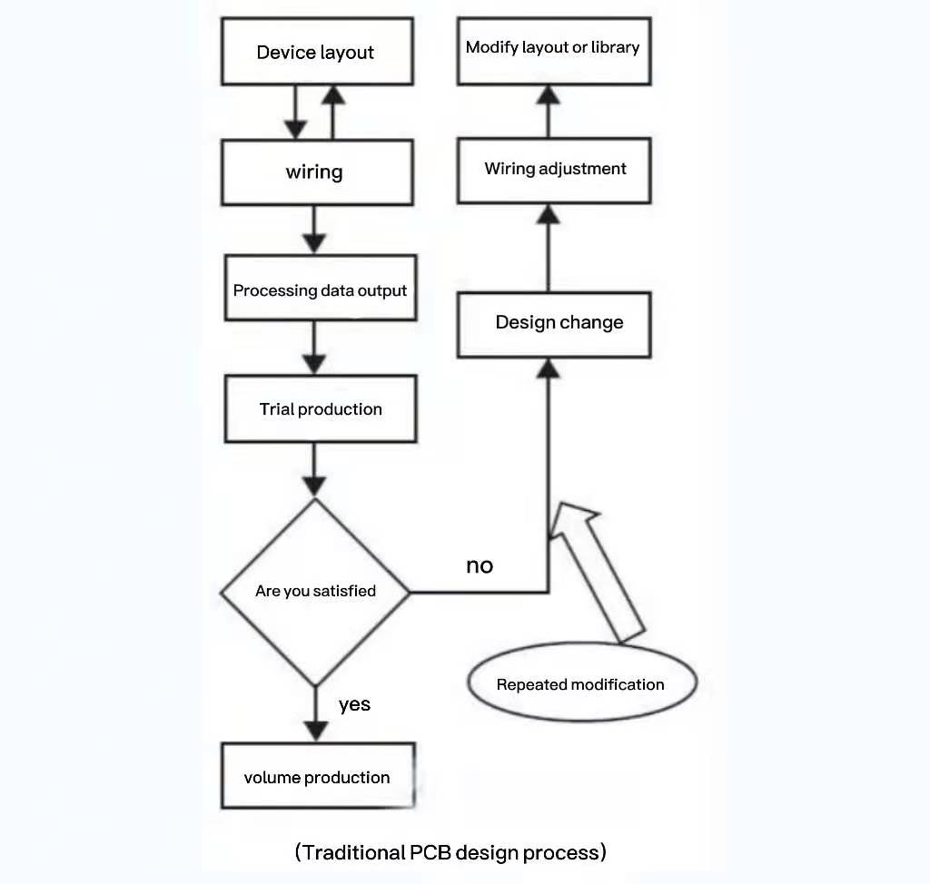
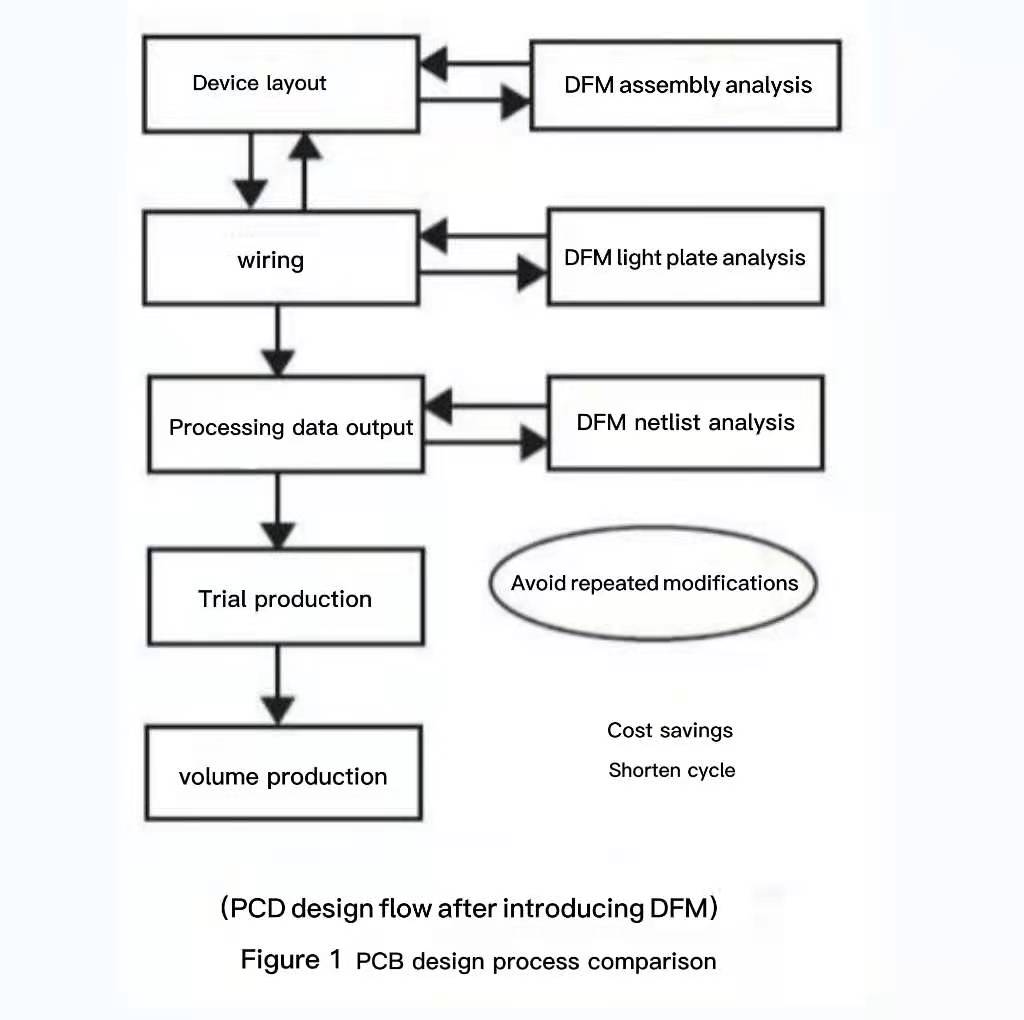
DFM technology concept
DFM technology, that is, manufacturability technology, mainly studies the relationship between the physical design of the product itself and the various parts of the manufacturing system, and uses it in product design to integrate the entire manufacturing system for overall optimization. DFM technology can reduce the development cycle and cost of the product, so that it can be put into production more smoothly. In other words, DFM is to find and solve problems early in the entire product life cycle.
2. DFM software application
Trilogy 5000 DFM analysis mainly includes light board manufacturing design analysis, assembly analysis and netlist analysis.
2.1 Preparation for analysis
The preparation of DFM analysis is very important, it is the basis of all analysis and a prerequisite for whether DFM analysis can proceed. The following five items are the main preparations.
2.1.1 Output ODB++ data generated by PCB design through EDA tool
ODB++ data is an industry standard data format. It combines traditional processing and assembly data such as PCB network information, stacking relationships, component information, printed board processing information, material information, and various production data including placement procedures and The test procedures etc. are gathered together. Generated by the ODB++ data generator embedded in the EDA design tool. Provide complete and true inspection basis for VALOR Trilogy 5000 DFM.
2.1.2 A complete BOM list based on each PCB design
Reading in the BOM list is to organize the BOM of the PCB design into a BOM format recognized by the VALOR Trilogy 5000 system, and correspond to the manufacturer and VPL package library of each device. The problem we encountered in mass production (traditional PCB design process) when corresponding to the BOM list is that the BOM automatically generated by our EDA tool is consistent with the company’s material procurement system, and the material procurement system is for readability. The name of the manufacturer of domestic devices is mostly reflected in Chinese, and the device model usually contains some marked Chinese. For the matching of the BOM list in the VALOR software, the link corresponding to the manufacturer cannot be achieved. Through repeated experiments, considering that the material code corresponds to each device, it will not happen that different devices use one material code, which is unique. Therefore, when interpreting the BOM, we set the attribute of the material code to MPN (Manufactor Part Number), and set the attributes of the two columns of manufacturer and device model to Describe, and set the code attribute of this unit to Manufactor( Manufacturer), there is only one manufacturer corresponding to all device models, which is the code name of the unit. After this is implemented, the steps of corresponding to the BOM list are greatly simplified, and many problems that have been plagued us, such as inaccurate manufacturer names and non-recognition in Chinese, which have been generated when corresponding manufacturers are cleverly avoided.
The process of reading in the BOM can verify the accuracy of the PCB design BOM list, and find early the phenomenon that the package used in the PCB design does not match the actual device library of the components, and generate a report of the inspection results, which is important for PCB design. Said it is a very good preliminary inspection process. If the company’s BOM format is certain, the process of reading the BOM can be simplified again by making a template.
2.1.3 Establish a VPL actual packaging library based on company material codes
By consulting the device manual, use the VALOR Trilogy 5000 library tool PLM to build the actual package library of each device. The VPL library contains the manufacturer's brand, specifications, and the actual package size of the components. VPL library is different from PCB design packaging library, it is a three-dimensional component packaging library that describes the actual size of components.
In the naming of the VPL package library, we use the VPL default naming method, but add the U_PCB_PACKAGE attribute to the package attribute, and write the value of this attribute into the EDA package name. The advantage of this is that when you click on the device you want to pay attention to during DFM analysis, you can intuitively see the name of the EDA package corresponding to this device, which facilitates the location and view of the package in question and saves time.
The establishment of the VPL package library is a process of gradual accumulation. You can start with resistors and capacitors. Use the COPYPART software provided by VALOR to organize a package of resistors or capacitors into an Excel table, and run through batch processing. The VPL package library of all the devices in the table can be built at one time. Of the thousands of packages in the EDA package library of general units, two-thirds of them should be composed of resistors and capacitors. If the above methods are used, the resistors and capacitors should be established first, which will lay a solid foundation and confidence for the establishment of the VPL library. ; Secondly, some important components such as connectors and CPUs should be established. This can ensure that after the assembly analysis of each printed board, the printed board put into production at least will not appear unusable; secondly, it should be established The VPL package of the more expensive devices guarantees the first success rate of the printed boards containing valuable devices. If the expensive devices are damaged during the assembly process due to packaging errors, it will be a big loss for the company. . Then set up the VPL library of commonly used devices. As the VPL library is gradually enriched, the VPL library is gradually established, so that most printed boards can be analyzed for assemblability.
2.1.4 Define the properties of the device
As the basis for all inspections, the establishment of an ERF rule management database is crucial. In the actual design and production, we have collected the manufacturing specifications of the printed board manufacturers, sorted out the design specifications and production process specifications of the design unit, analyzed and compared one by one, and established an ERF rule management database that conforms to our company. It is gradually improved in practice. The ERF rule management library includes the light board analysis rule management library and the assembly analysis rule management library.
2.2 Design for assemblability
When the PCB layout of the printed board is basically completed:
1) Import ODB++ data;
2) Import the BOM list of the design;
3) Call the VPL actual packaging library and ERF assembly analysis rule management library corresponding to the established material code;
4) According to different printed board assembly requirements, set up the corresponding assembly process, and divide the process area for the printed board;
5) Define device attributes;
6) Perform assembly inspection, generate visual graphics, and automatically generate assembly analysis reports.
Assemblability inspection includes inspections such as component packaging inspection, marking point inspection, component analysis, pad analysis, pad and pin correspondence analysis, test point analysis, and template opening analysis. The above inspection items all include sub-items. For example, component analysis includes component spacing, component direction, component height, component silk screen, and component forbidden area. Through inspection, it can be seen that the components and PCB pads do not match, component collision interference, and component soldering problems.
With the increasing complexity of PCB design, a printed board will contain thousands of devices, and the interposing devices and surface mount devices are very densely distributed. After the layout of the printed board is completed, thousands of Adjusting the silk screen of various devices is also a lot of work, and this kind of complicated work will inevitably lead to unreasonable or even upside-down position of the tag. The ordinary EDA design software does not provide check items for this kind of problem, so once this kind of problem occurs, it is often found after debugging after the printed board is processed and the device is installed. It brought a lot of trouble to the later assembly and debugging, delayed the progress of product research and development, and brought economic losses. Through component analysis, the problem of bit number misalignment shown in Figure 2 can be easily checked out. It replaces the manual inspection process of PCB designers, improves efficiency, and guarantees the quality of our PCB design. This inspection is very meaningful for our PCB design.
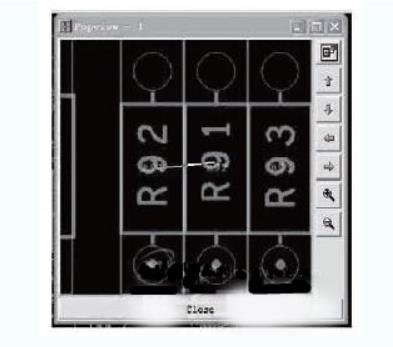
Figure 2 Bit number misalignment
Component spacing analysis provides a method for the inspection of too close device spacing that we often encounter in PCB design. The spacing requirements between different components are different, and the height is also different, which can be set through the correspondence table of ERF and device properties. By calling the VPL library, we analyze whether the different spacings of various components meet the requirements. As shown in Figure 3, the distance between the two components is too close, which leads to insufficient tin on the pins of short components due to the difference in height of the two components during wave soldering, which can cause empty soldering or virtual soldering.
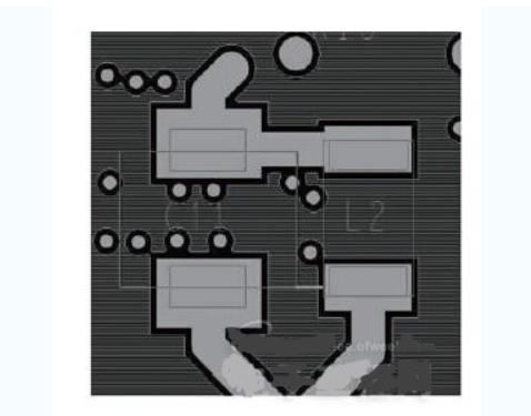
Figure 3 The distance between the two components is too close
The component packaging analysis is mainly to check the correctness of the component packaging on the PCB. This inspection is particularly important. In the PCB design, the component package corresponding error or the package library establishment error directly causes the processed printed board to be unusable, and it has to be re-produced. This not only wastes costs, reduces efficiency, but also loses market competitiveness.
As shown in Figure 4, the gray box is the actual device size of the VPL library. Compared with the black PCB design data below, it is obvious that the package pad design is unreasonable, the pad welding part is reserved too short, and the pad width is not enough, which is easy to cause Welding during the welding process.
Through the application of assemblability analysis, the accuracy of PCB design is improved. Since we have incorporated many processing requirements of the processing manufacturer into the ERF rules, the number of back and forth communication with the processing manufacturer has been reduced, and the efficiency and the first-time success rate of the printed board production have been improved.
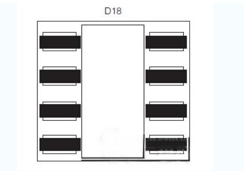
Figure 4 Unreasonable pad design
2.3 Netlist analysis
When the PCB layout is completed, the ODB++ data generated during the design is extracted, and the netlist is analyzed. By comparing the standard network, the design error (open circuit or short circuit) of the network integrity will be directly identified in the graph. Even the open circuit and short circuit of the power ground can be accurately reported by the inspection mode converted to Pin-Point. This function can help PCB inspectors find the problem of incomplete PCB inspection caused by insufficient experience, so that PCB inspectors can verify the final design data integrity before the product is put into production.
2.4 Light board analysis
According to ERF's light board analysis rule management library, extract the ODB++ data generated by the PCB design to check the manufacturability of the PCB light board. PCB light board analysis mainly includes drilling analysis, signal analysis, power layer analysis, solder mask analysis and silk screen analysis.
Because different PCB designers have different design levels and methods, in the PCB design process, due to different experiences, the rules for setting up layout and routing are different, and the quality of the design is also very different. How to make the PCB quality is controlled. We will reflect all the design requirements and specifications in the inspections of the light board analysis by setting the ERF light board analysis rule management library.
For example, in PCB design, the size of the heat-insulating faceplate should be set according to the power requirements of different power sources. If the heat-insulating faceplate is too small or blocked, it will cause too fast heat dissipation during welding, poor solderability, and the connection cannot meet the power requirements, etc. Problem. However, as long as the PCB design software meets the connection line width requirement, it will not prompt an error.
As shown in Figure 5, it is the case that the heat-insulating faceplate is too small. The optical panel analysis will check according to the setting of the ERF rules, and the classification prompts whether it meets the requirements of heat dissipation and connection power, and avoids errors caused by factors such as experience.
Application of DFM technology in PCB design
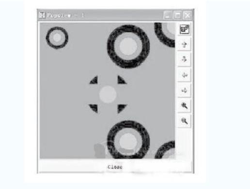
Figure 5 The heat-insulating faceplate is too small
In addition, our PCB design tool only provides inspection items between printed lines and pads, and does not provide inspection of the distance between printed lines and solder mask. As shown in Figure 6, after optical board analysis, it can be found that the printed lines are too close to the solder mask, which avoids the copper leakage of the printed lines produced, and the oxidation of copper will directly affect the quality of the signal. These quality problems that may be exposed after a long time of use should also be considered when we check the PCB.
Application of DFM technology in PCB design
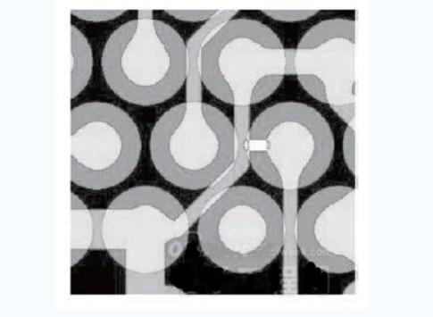
Figure 6 The wire is too close to the solder mask
In light panel analysis, if you copy each inspection step into a checklist (Checklist), you can simplify the operation of each inspection. You can also specify shortcut keys, and you can perform light panel analysis by pressing a button, which greatly reduces the workload of inspection .
2.5 Software synchronization
Once the EDA database is read as ODB++, Trilogy 5000 can provide intelligent graphics to connect to the EDA tool. Using the shortcut keys set by the software, the designer can directly synchronize from the Trilogy5000 screen to the same frame and location displayed on the EDA tool, which provides us with great convenience in finding the error point in the EDA tool quickly and easily.
3. The difference between DFM software and PCB design software rule checking function
DFM software tools are based on actual production rules, while PCB design software checks are only based on design rules, which are tools in two different fields.
The analysis in the PCB design software is generally applied to the design department, and the data is checked at the back end of the design to ensure that there are no problems that violate the electrical rules, focusing on the realization of logic functions; DFM is applied to the process department and the production assembly department to ensure the design The data meets all the requirements of manufacturing, assembly and testing.
The function of manufacturability analysis of related modules in PCB design software is relatively simple, and the rules are not rich enough. Tools such as assemblability analysis and testability analysis are not available.
4. Conclusion
DFM software provides us with a comprehensive PCB design automation review program, which makes our products more standardized. Even with different PCB design software and PCB designers with different experience, the quality of products designed by PCB designers is guaranteed. Make process review participate in all stages of product design in parallel, solve and discover all hidden manufacturability quality hazards in the design stage, and greatly improve the quality of our PCB design. The efficiency of printed circuit board processing, process management and electrical equipment process has been greatly improved, the quality of the product has been improved, the cost of the product and the development cycle have been reduced, and the competitiveness of the product has been increased.
In addition, the application of DFM software is also conducive to the standardization of processes. Through DFM specifications, the design and manufacturing departments are organically linked, and at the same time, the standardization of production test equipment is achieved. Based on the current trend of product manufacturing outsourcing, it will be possible to realize the specialized transfer of product technology, which is conducive to the realization of greater development of enterprises.