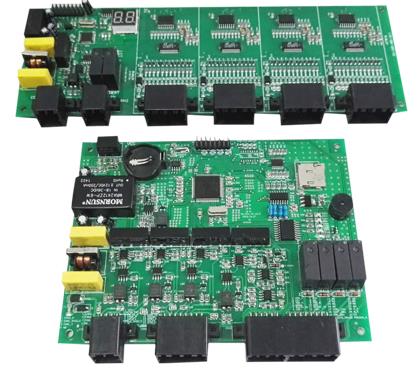
The solution to the PCB circuit board laminate problem is here
I think the PCB circuit board laminate problem has puzzled everyone for a long time. After discussing with the engineer for a long time, I was able to write this article. The editor of the circuit board factory cites some common problems and related solutions of PCB laminates. If you encounter common problems such as PCB board laminates, you should formulate a normative standard, and then you can prescribe the right medicine for such problems in the future.
1. The flow direction should be scientific and reasonable
There are many aspects involved in this point, such as high voltage/low voltage, input/output, strong/weak data signal, high frequency/low frequency, and so on. The most reasonable flow of them should be linear and should not merge with each other. The principle is to eliminate mutual interference. The more appropriate flow direction is in a straight line, but it is difficult to achieve. The most improper flow direction is loop. Fortunately, there is also an isolation operation. If it is specifically for direct current, the low-voltage PCB circuit board design requirements can be lower. Therefore, the so-called "scientific rationality" is only relative.
2. Reasonable layout of power filter/decoupling capacitors
The layout of the PCB circuit board is critical to the appearance and performance of the entire circuit board. Only part of the power supply filter/decoupling capacitors will be drawn in the schematic, but it is not clearly pointed out where they should be connected. I think those capacitors are set for switching devices or other components that require filtering/decoupling. The position of the capacitors must be close to those components, and the effect will not be found if they are separated far away. When we scientifically and rationally use power filter/decoupling capacitors, the common problems of grounding points no longer seem to be prominent. You can try it out!

3. Good grounding point
I don't need to say more about the importance of choosing the grounding point. Countless professionals have discussed it, and generally speaking, standards are required to be common. For example, the multiple ground wires of the forward amplifier should be merged and then connected to the main ground and so on. However, in real life, it is difficult to do it completely due to various types of restrictions. But we cannot ignore it, and should do our best to follow the principles. This common problem is very flexible in actual situations, and different people have different solutions. It is very easy to understand if it can be expressed specifically for specific PCB circuit boards.
4. Reasonable line selection
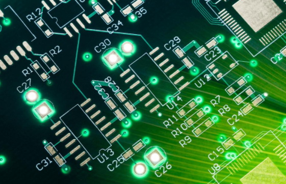
They are all called circuit boards, and lines are of course very important! When conditions permit, try to make the line wider. The high-voltage and high-frequency cables should be smoother, without sharp chamfers. It should not be 90° in the corners, and the ground wire should be as wide as possible. To solve the problem of the grounding point, a better way is to cover a large area of copper. If there is a better way to leave a comment in the comment area, I will also learn more.
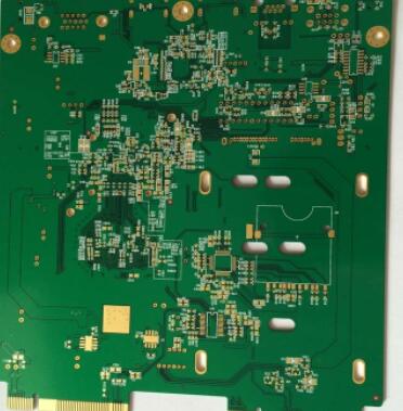
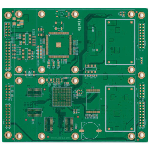
The problem of PCB circuit board is inseparable from design and circuit board processing. For example, sometimes the problems that appear in post-production are likely to be caused by the design of the PCB circuit board. For example, too many wire holes, substandard copper sinking process, etc., can easily hide a lot of potential safety hazards. We can draw a conclusion from the above-mentioned problems, in the PCB circuit board design conception should reduce as much as possible via holes. If the number of parallel lines in the same direction is large and the density is high, they will be connected together during welding. Therefore, the welding level during production determines the linear density. If the distance between the solder joints is too small, the difficulty of manual soldering will increase a lot. At this time, the only way to solve the welding quality is to reduce the work efficiency. Otherwise, there will be more and more problems in the future, and it will become more and more difficult to deal with. The level and efficiency of the welder determines the narrowest pitch of the solder joints.
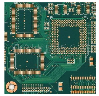
When the size of the pad or the wire hole is too small, it becomes more difficult for manual drilling. When the size of the pad does not match the size of the drilled hole, it is a thunderbolt for CNC drilling, and the pad is likely to take a C-shape. If the situation is serious, the pad will be drilled out. If the wire is too thin, and the large-scale unwiring area has no copper, uneven corrosion is likely to occur. That is to say, when the unwiring area is etched, the thin wires are likely to be excessively corroded. Sometimes it seems that the line is broken but it is not broken. If it is more serious, it will be broken. Therefore, setting copper is not only to expand the ground area.