With the rapid increase in speed requirements in recent years, new bus protocols continue to propose higher speeds. The traditional bus protocol can no longer meet the requirements. The serial bus is favored by many designers because of its better anti-interference, fewer signal lines, and higher speed. And the serial bus is especially the way of differential signal is the most. So in this article I have sorted out some design of differential signal lines and discussed it with everyone.
1. The principle, advantages and disadvantages of differential signal lines
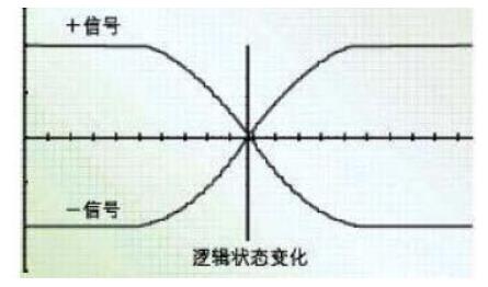
Differential signal (Differential Signal) is more and more widely used in high-speed circuit design. The most critical signal in the circuit is often designed with a differential structure. What makes it so popular? How to ensure its good performance in PCB design? With these two questions, we proceed to the next part of the discussion. What is a differential signal? In layman's terms, the driving end sends two equal and inverted signals, and the receiving end judges the logical state "0" or "1" by comparing the difference between the two voltages. The pair of traces carrying differential signals is called differential traces.
Compared with ordinary single-ended signal traces, differential signals have the most obvious advantages in the following three aspects:
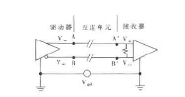
a. Strong anti-interference ability, because the coupling between the two differential traces is very good. When there is noise interference from the outside, they are almost coupled to the two lines at the same time, and the receiving end only cares about the difference between the two signals. Therefore, the external common mode noise can be completely canceled.
b. It can effectively suppress EMI. For the same reason, due to the opposite polarity of the two signals, the electromagnetic fields radiated by them can cancel each other. As shown in the figure, the current in AA' is from right to left, and the current in BB' is from left to left. Right, then according to the right-hand spiral rule, their magnetic lines of force cancel each other out. The tighter the coupling, the more magnetic lines of force cancel each other out. The less electromagnetic energy is released to the outside world.
c. The timing positioning is accurate. Because the switch change of the differential signal is located at the intersection of the two signals, unlike the ordinary single-ended signal, which depends on the high and low threshold voltages to determine, it is less affected by the process and temperature, which can reduce the error in the timing., But also more suitable for low-amplitude signal circuits. The current popular LVDS (low voltage differential signaling) refers to this small amplitude differential signaling technology.
2. An example of differential signal: LVDS
LVDS (Low Voltage Differential Signaling) is a low-swing current-type differential signal technology, which enables signals to be transmitted on differential PCB wire pairs or balanced cables at a rate of several hundred Mbps, and its low-voltage amplitude and low-current drive output are realized In order to achieve low noise and low power consumption. The LVDS driver consists of a current source that drives a differential line pair. The current is usually 3.5mA). The LVDS receiver has a very high input impedance, so most of the current output by the driver flows through a matching resistance of 100Ω‧ and is connected to the receiver. The input terminal generates a voltage of about 350mA. When the driver flips, it changes the direction of current flowing through the resistor, thus producing valid logic "1" and logic "0" states. The low-swing drive signal realizes high-speed operation and reduces power consumption, and the differential signal provides a low-voltage swing with appropriate noise margins and greatly reduced power consumption. The substantial reduction in power allows multiple interface drivers and receivers to be integrated on a single integrated circuit. This improves the efficiency of the PCB board and reduces the cost.
Regardless of whether the LVDS transmission medium used is a PCB wire pair or a cable, measures must be taken to prevent the signal from being reflected at the medium terminal and reduce electromagnetic interference at the same time. LVDS requires the use of a termination resistor (100±20Ω) that matches the medium. This resistor terminates the circulating current signal and should be placed as close as possible to the input of the receiver. The LVDS driver can drive twisted pair at a speed of more than 155.5Mbps over a distance of more than 10m. The actual limit on the speed is: 1. The speed of TTL data sent to the drive; 2. The bandwidth performance of the medium.
Usually a multiplexer is used on the driver side and a demultiplexer is used on the receiver side to implement multiplexing conversion of multiple TTL channels and one LVDS channel to increase the signal rate and reduce power consumption. And reduce the transmission medium and the number of interfaces, and reduce the complexity of the equipment.
The LVDS receiver can withstand at least ±1V of the ground voltage change between the driver and the receiver. Since the typical bias voltage of the LVDS driver is +1.2V, the sum of the ground voltage change, the driver bias voltage, and the lightly coupled noise, the input of the receiver is a common-mode voltage with respect to the receiver's ground. The common mode range is: +0.2V~+2.2V. It is recommended that the input voltage range of the receiver is: 0V~+2.4V.
3. Wiring requirements for differential signals:
For PCB engineers, the most concern is how to ensure that these advantages of differential wiring can be fully utilized in actual wiring. Perhaps anyone who has been in contact with Layout will understand the general requirements of differential wiring, that is, there are two points to pay attention to in the wiring of differential pairs. One is that the length of the two wires should be as long as possible, and the equal length is to ensure the timing of the two differential signals. Keep the opposite polarity and reduce the common mode component. The other is that the distance between the two wires (this distance is determined by the differential impedance) must be kept constant, that is, it must be kept parallel. There are two parallel ways, one is that the two wires run on the same side-by-side, and the other is that the two wires run on two adjacent layers above and below (over-under). Generally, the former has more side-by-side implementations.
The equidistance is mainly to ensure the same differential impedance between the two and reduce reflection. The wiring method of the differential pair should be close and parallel appropriately. The so-called appropriate proximity is because the distance will affect the value of differential impedance, which is an important parameter for designing differential pairs. The need for parallelism is also to maintain the consistency of the differential impedance. If the two lines are suddenly far and near, the differential impedance will be inconsistent, which will affect the signal integrity and timing delay.
Below is the differential transmission line model
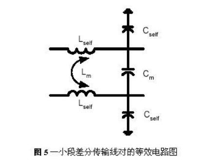
To facilitate analysis, a differential line pair is often described in terms of its odd-mode and even-mode impedance and delay, and these parts corresponding to its differential mode and common mode are closely related, so it can be calculated by Equation 1.
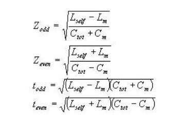
Here Ctot = Cself + Cm. Cself is the capacitance between one line and ground, and Cm is the capacitance between two lines. Lself and Lm are the self-inductance of one line and the mutual inductance between two lines, respectively.
Differential impedance is defined as the impedance measured between two differentially driven wires. (The so-called differential drive means when two signals are exactly the same but opposite in polarity). Differential impedance refers to the odd-mode impedance. The so-called odd-mode impedance refers to the impedance of a transmission wire in a differential pair when two wires are driven differentially [3]. Even mode impedance refers to the impedance of two wires in a differential pair when both wires are driven by a single common-mode signal to ground.
Using Equation 1, it can be derived: differential impedance

Common mode impedance

But all these rules are not used to mechanically apply, and many engineers seem to still not understand the essence of high-speed differential signal transmission. The following focuses on several common misunderstandings in PCB differential signal design.
Misunderstanding 1: It is believed that the differential signal does not need a ground plane as a return path, or that the differential traces provide a return path for each other. The reason for this misunderstanding is that they are confused by superficial phenomena, or the mechanism of high-speed signal transmission is not deep enough. Although the differential circuit is insensitive to similar ground bounces and other noise signals that may exist on the power and ground planes. The partial return cancellation of the ground plane does not mean that the differential circuit does not use the reference plane as the signal return path. In fact, in the signal return analysis, the mechanism of differential wiring and ordinary single-ended wiring is the same, that is, high-frequency signals are always Reflow along the loop with the smallest inductance, the biggest difference is that in addition to the coupling to the ground, the differential line also has mutual coupling. Which kind of coupling is strong, which one becomes the main return path.
In PCBcircuit design, the coupling between differential traces is generally small, and often only accounts for 10-20% of the coupling degree, and more is the coupling to the ground, so the main return path of the differential trace still exists on the ground plane . When there is a discontinuity in the ground plane, the coupling between the differential traces will provide the main return path in the area without a reference plane. Although the influence of the discontinuity of the reference plane on the differential trace is not as serious as that of the ordinary single-ended trace, it will still reduce the quality of the differential signal and increase EMI, which should be avoided as much as possible. Some designers believe that the reference plane under the differential trace can be removed to suppress some common mode signals in differential transmission. However, this approach is not desirable in theory. How to control the impedance? Not providing a ground impedance loop for the common mode signal will inevitably cause EMI radiation. This approach does more harm than good.
So keep the PCB ground plane return path wide and short. Try not to cross islands (across the separated areas of adjacent power supplies or ground layers.) For example, USB, SATA, and PCI-EXPRESS in motherboard design are best not to cross islands. Ensure that there is a complete ground plane or power plane under these signals.
Misunderstanding 2: It is believed that keeping equal spacing is more important than matching line length. In actual PCB layout, it is often not possible to meet the requirements of differential design at the same time. Due to the existence of factors such as pin distribution, vias, and wiring space, the purpose of line length matching must be achieved through proper winding, but the result must be that some areas of the differential pair cannot be parallel. In fact, the spacing is unequal. The impact of is minimal. In comparison, the line length mismatch has a much greater impact on the timing. From the theoretical analysis, although the inconsistent spacing will cause the differential impedance to change, because the coupling between the differential pair itself is not significant, the impedance change range is also very small, usually within 10%, which is only equivalent to one pass. The reflection caused by the hole will not have a significant impact on signal transmission. Once the line length does not match, in addition to the timing offset, common mode components are introduced into the differential signal, which reduces the quality of the signal and increases EMI.
It can be said that the most important rule in the design of PCB differential traces is the matching line length, and other rules can be flexibly handled according to design requirements and actual applications. At the same time, in order to compensate for the impedance matching, a matching resistance can be added between the differential line pairs at the receiving end. Its value should be equal to the value of differential impedance. This way the signal quality will be better.
Therefore, the following two points are recommended:
(A) Use terminal resistance to achieve the maximum matching to the differential transmission line, the resistance value is generally between 90 ~ 130 Ω, the system also needs this terminal resistance to generate a normal working differential voltage;
(B) It is best to use surface mount resistors with an accuracy of 1-2% across the differential line. If necessary, two resistors with a resistance of 50Ω each can be used, and a capacitor is grounded in the middle to filter out the common mode. Noise.
Generally, the matching requirements for the CLOCK of the differential signal and the like are equal to within +/-10mils.
Misunderstanding 3: Think that the differential wiring must be very close. Keeping the differential traces close is nothing more than to enhance their coupling, which can not only improve immunity to noise, but also make full use of the opposite polarity of the magnetic field to offset electromagnetic interference to the outside world. Although this approach is very beneficial in most cases, it is not absolute. If we can ensure that they are fully shielded from external interference, then we do not need to use strong coupling to achieve anti-interference. And the purpose of suppressing EMI. How can we ensure good isolation and shielding of differential traces? Increasing the spacing with other signal traces is one of the most basic ways. The electromagnetic field energy decreases with the square of the distance. Generally, when the line spacing exceeds 4 times the line width, the interference between them is extremely weak. Can be ignored. In addition, isolation by the ground plane can also play a good shielding role. This structure is often used in the design of high-frequency (above 10G) IC package PCBs. It is called a CPW structure, which can ensure strict differential impedance. Control (2Z0).
Differential traces can also run in different signal layers, but this method is generally not recommended, because the differences in impedance and vias produced by different layers will destroy the effect of differential mode transmission and introduce common mode noise. In addition, if the adjacent two layers are not tightly coupled, it will reduce the ability of the differential trace to resist noise, but if you can maintain a proper distance from the surrounding traces, crosstalk is not a problem. At general frequencies (below GHz), EMI will not be a serious problem. Experiments have shown that the attenuation of radiated energy at a distance of 500 mils from differential traces has reached 60 dB at a distance of 3 meters, which is enough to meet the FCC electromagnetic radiation standards, so The designer does not have to worry too much about the electromagnetic incompatibility caused by insufficient differential line coupling.
4. Eye diagram
In the test of differential signals, we often encounter a test item is the eye diagram, and many design beginners may have heard of the eye diagram test. But there are still many who don't know how the eye diagrams come from. Learning to look at the eye diagram is very useful for your own testing and DEBUG. The following describes the eye diagram.
In every clock cycle there will be a signal in the transmission. But if it is a very long bit stream (bits), then it is difficult to determine whether the signal meets the specifications (specifications). In order to facilitate the analysis, if all the signal bits can form a signal graph, then you can look at this and superimpose these graphs to see if they meet the specifications. This is the eye diagram.
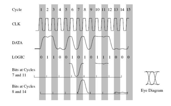
As shown in the figure below, it is assumed that all signals are triggered on the rising edge of the clock. Then the waveforms of all data signals are taken out according to the rising edge and superimposed together. Each such waveform is called a SYMPLE. As shown in the picture (only one waveform is taken out on the picture so that the reader can see it clearly), this forms the first half of the eye diagram. Then take them out according to the falling edge and stack them together, then the second half of the eye diagram can be formed. At the same time, high-level or low-level signal waveforms form the top and bottom of the eye diagram. This forms a standard eye diagram (as shown below). Then all you have to do is to define it in the eye diagram according to the signal specification.
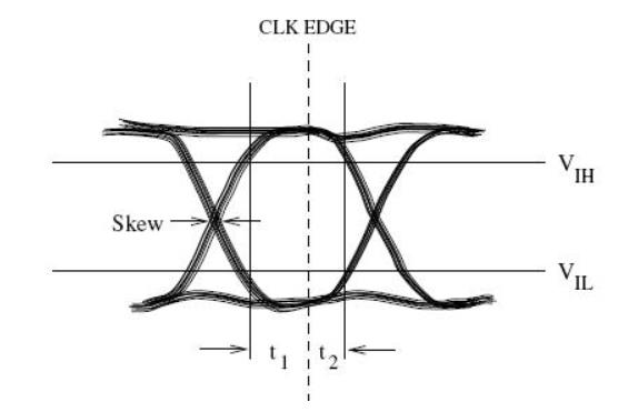
Of course, the following figure also shows CLK, the actual serial differential signal cannot detect CLOCK on the signal line.
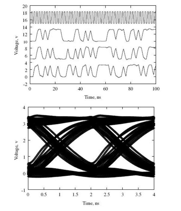
Let's take an example. From the eye diagram, the signal quality is very poor. Corresponding to its SYMPLE, it can be seen that the signal quality is very poor. The rising and falling edges are too slow, the consistency is too poor, the HIGH LEVEL of the signal is not enough, and the SKEW is too large.
5. Measurement of differential signal.
Input connection Generally speaking, the interconnection between a differential amplifier or probe and a signal source is the biggest source of error. In order to maintain input matching, the two channels should be as the same as possible. Any wiring of the two input terminals should have the same length. If a probe is used, its model and length should also be the same. When measuring low-frequency signals with high common-mode voltages, avoid using probes with attenuation. At high gains, such probes cannot be used at all, because it is impossible to precisely balance their attenuation. When high voltage or high frequency applications require attenuation, special passive probes specially designed for differential amplifiers should be used. This kind of probe has a device that can precisely adjust the DC attenuation and AC compensation. In order to obtain the best performance, each specific amplifier should have a dedicated set of probes, and the amplifier should be calibrated according to the procedures attached to this set of probes.
A common method is to twist the + and-input cables in pairs. This reduces the possibility of picking up line frequency interference and other noise. If you want to capture the eye diagram, you should consult the instrument manufacturer to obtain the latest software and fixtures. Generally, this set of software and fixtures are charged separately