At low frequencies, the via hole has little effect. But in the high-speed series connection, the via hole will ruin the entire system.
In some cases, at 3.125Gbps, they can use a nice, wide aperture. Turn it into a pillar at 5 Gbps. Understanding the root cause of the limitation of vias is the first step in optimizing their design and verifying them.
This article will describe a simple via-hole modeling and simulation process, from which you can get some key points for optimal design.
You can't happen to design an interconnect that can work at 2Gbps or higher. In order to achieve the target data transfer rate, the interconnection must be optimized. In many cases, vias may become the end of high-speed series connection, unless vias are optimized to make their impact smaller.
The root cause of the differential via problem mainly comes from three aspects, 90% is the viastub, 9% is from the vias, and the other 1% is from the return vias. The so-called via process is to solve these three key points.
The first step is to minimize the length of the through-hole root. As a rule of thumb, the length of the via root, in mils, should be less than 300 mils/BR, and Br is the Gbps rate.
The second step is to make the penetrating part of the hole path close to the impedance of the line, which is usually 100 ohms. The impedance difference of different vias is usually less than 100 ohms. Therefore, if possible, try to reduce the diameter, increase the spacing, clear the holes, increase the through holes on the layer, and remove all useless pads. In addition, the surrounding line impedance can be reduced. Generally, even a 65 ohm impedance difference will result in an insertion loss of less than -1 dB, let alone a 15GHz, 100 ohm difference system.
Finally, placing adjacent return vias near the signal space will help control the signal noise generated by the transmission of ordinary signals in the system. For different systems, the introduction of return via is not necessarily critical to signal quality, although this is always a good habit.
Once these key points are optimized, considering the real situation, we always have the same problem, will it operate normally? Have I done enough in the process of processing vias?
One way to answer this question is to set up a test device and perform measurements. This is the "test performance" approach. The cost is very high, time-consuming and resource-consuming, but the end result will be your confidence in greatly improving product reliability. Another method is to simulate the final design before determining the hardware and submitting it for construction.
The only way to accurately simulate differential vias is to use 3D full-wave electromagnetic field solvers, such as those provided by Agilent Technologies and CST. These tools have been proven to be very accurate, and it is easy to explain the different and common effects, including those from the return path, but they are generally more complex. The S-number representation module of this tool can be used in many system simulators to predict the first and second level effects. This is a perfect process.
However, for some via structures, the differential impedance characteristics can be approximated with a very simple module. In this way, the analysis prefab can be shortened to minutes instead of hours or even days. It can also analyze in depth how many possible problems the vias will face, and the characteristics that are relatively important for the design. Therefore, when evaluating the via effect in high-speed series, we always use a simple model first. Relative to the energy invested, the return is huge.
First, the differential via can be simulated as a unified differential pair with differential impedance and dielectric constant. It is divided into two or three equal parts, depending on how the signal layer enters and leaves the via. The only difference in these parts is their length. They all have the same differential impedance or odd mode impedance, and dielectric constant.
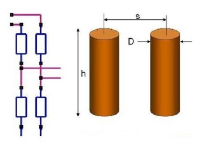
The differential impedance of the two vias can be roughly estimated based on the typical impedance analysis model of twin rods. As shown in Figure 1

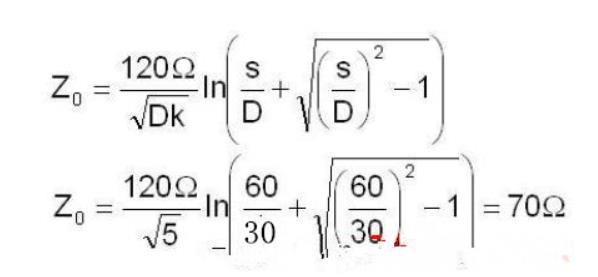
The differential impedance can be estimated by the twin rod model:

Z0 = differential impedance (ohm)
D = diameter of via hole (mils)
s = center to center distance (mils)
Dk = effective dielectric constant is about 4-6.5
For example, if the dielectric constant of glass weave and resin is 5, the gap is 60 mils, and the diameter of the via is 30 mils, then the differential impedance is:
The vias are generally less than 100 ohms. What kind of value is acceptable to us? The most common answer to the signal integrity question is, "It depends." If the insertion loss of -1dB is acceptable, then the impedance of the via can be as low as 65 ohms, but it can still be satisfied in a 100 ohm environment This performance specification.
Generally speaking, only using this electrical model to simulate the entire link will give you a confident answer. This simple differential pair model is a necessary element to establish confidence in your design before you manufacture it.