In the designof high-speedPCB, a large part of the work is to carry out the noise budget and plan the noise level generated by various noise sources of the system. This involves a very basic but very important concept: voltage tolerance.
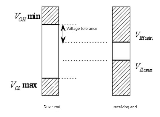
Voltage tolerance refers to the worst-case sensitivity difference between the output of the driver and the input of the receiving end. Many devices are input voltage sensitive. The figure shows the logical relationship between the driver output and the receiver input voltage.

For the driver end, the output high level is not lower than VOH min, and the output low level is not higher than VOL max. As for the input at the receiving end, as long as it is higher than VIH min, it can guarantee that logic 1 is received reliably, and as long as it is lower than VIL max, it can be guaranteed to receive logic 0. If the input voltage is in the region between VIH min and VIL max, it may be judged as 1 or 0 by the receiving circuit. Therefore, the input voltage cannot be in this uncertain region for the receiving circuit. In terms of the relationship between high-level output and input, there is a difference between the minimum output value and the minimum allowable input value. This value is the high-level voltage tolerance.
That is: high-level voltage tolerance = VOH min-VIH min. Similarly, the low-level voltage tolerance = VIH min-VILmax.
Voltage tolerance provides a buffer zone for various undesirable factors in the processing circuit system, so that the system can tolerate signal distortion in the sending and receiving process to a certain extent. Voltage tolerance plays an important role in the system noise budget design. The final total noise of the system cannot exceed the voltage tolerance, otherwise, the system will not work normally when the signal enters the uncertain region of the receiving end.
There will always be unsatisfactory factors in the actual system, which will cause signal degradation and introduce noise. The following situations will introduce noise:
1. Due to the existence of loop impedance, a voltage drop will inevitably occur in the loop, resulting in a ground potential difference between logic devices. The signal sent by the gate circuit is a fixed potential on the local ground potential. If there is an offset between the reference potential of the sending end and the receiving end, then the received potential will be another potential.
2. The threshold level of some logic products is a function of temperature. Signal transmission from a gate with a lower temperature to a gate with a higher temperature may have reduced tolerance or a negative tolerance.
3. The rapidly changing return signal current flows through the ground path inductance, causing the voltage to ground between logic devices to change. These ground voltage differences have the same effect on the received signal potential as the DC ground potential difference mentioned above. This is a form of perceptual crosstalk.
4. The signals on adjacent lines may be coupled with each other through their mutual capacitance or mutual inductance, which may cause crosstalk to a specified line. Crosstalk is superimposed on the expected received signal, which may shift a good signal to an adjacent switching threshold.
5. Ringing, reflections, and long lines distorted the shape of the binary signal. Compared with the transmitting end, the changed signal at the receiving end appears smaller (or larger). Tolerance provides some tolerance for signal distortion.
The first two situations will exist in all electronic systems, regardless of their operating speed. The latter three are unique to high-speed systems. These three high-speed effects all change with the size of the transmitted signal: the greater the signal return current, the higher the ground potential difference caused. The greater the signal voltage (or current), the more crosstalk will be generated, and the greater the transmission signal, the more serious the ringing and reflections will be. Therefore, no matter it is a low-speed or high-speed system, noise is inevitably introduced, and the voltage tolerance gives the system room for adjustment.