At present, the related signal integrity (SI) engineering and research at home and abroad is still an immature subject, and its analysis methods and practices are not well perfected, and it is still in the stage of continuous exploration. In the PCB design method based on signal integrity computer analysis, the most core part is the establishment of the PCB board-level signal integrity model, which is the main difference from the traditional design method. The accuracy of the SI model will determine the correctness of the design, and the buildability of the SI model determines the feasibility of this design method.
The problems in high-speed digital circuit design are prominently reflected in the following types: (1) The increase in operating frequency and the reduction of signal rise/fall time will reduce the timing margin of the design system and even cause timing problems; (2) Transmission line effects The resulting signal oscillation, overshoot and undershoot will all pose a great threat to the fault tolerance, noise tolerance and monotonicity of the designed system; (3) After the signal edge time drops to 1 ns, the crosstalk between the signals becomes very serious. An important problem; (4) When the time of the signal edge is close to 0.5ns, the stability problem of the power system and the electromagnetic interference (EMI) problem also become very prominent.
In a high-speed system, whether the signal interconnection of the system can be handled well and the problem of signal integrity can be solved is the key to the success of the system design. At the same time, signal integrity is also the basis and prerequisite for solving power integrity, electromagnetic compatibility and electromagnetic interference (EMC/EMI) issues.
High-frequency effects and transmission line theory
High frequency effect
In the case of high-frequency skin effect, electromagnetic waves will attenuate sharply when entering a good conductor. Even at a distance less than one wavelength in a good conductor, the electromagnetic wave has been significantly attenuated, so high-frequency electromagnetic fields can only exist on one surface of a good conductor. In the thin layer, this phenomenon is called skin effect. The depth of the electromagnetic wave field intensity attenuation to 1/e of the surface is the skin depth
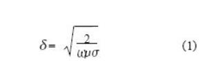
Formula (1) explains: the greater the electrical conductivity, the better the electrical conductivity, the higher the working frequency, the smaller the skin depth, which causes the resistance at high frequencies to be much greater than the resistance at low frequencies or DC. When the proximity effect is in the mutual electromagnetic interference between several current-carrying conductors, the current distribution of the cross-section of each current-carrying conductor is different from that of an isolated current-carrying conductor. When there are two adjacent conductors carrying currents in opposite directions, the current density is the largest at the closest points on the two sides that are close to each other; when the current directions of the two current-carrying conductors are the same, the current density on the two outer sides is the smallest. In general, the proximity effect increases the equivalent resistance and decreases the inductance.
Transmission line theory
A generalized transmission line is a conductor, medium, or a guiding system composed of them that guides the transmission of electromagnetic waves in a certain direction. The transmission line generally discussed refers to the microwave transmission line, and its theory is the long-line theory. When the geometric size of the transmission line is comparable to the wavelength of the electromagnetic wave, the distribution parameters (or parasitic parameters) of the transmission line must be considered. In high-speed digital or radio frequency circuit design and high-speed circuit simulation design, many electromagnetic phenomena must be explained using transmission line theory. Transmission line theory is the basis for studying high-speed digital (or radio frequency) circuits.
Basic transmission line theory When the transmission signal rate or frequency reaches a certain level, the distribution parameters on the transmission signal channel must be considered. Taking parallel double wires as an example, the skin effect on them increases the RF impedance per unit length. When it reaches the radio frequency range, the magnetic field around the parallel double lines is very strong, and its parasitic inductance must be considered, and the electric field between the parallel double lines should be equivalent to a capacitor. At the same time, the leakage phenomenon between the wires should be considered when the frequency is high. So the equivalent circuit of a unit length transmission line can be composed of R, L, G, C 4 elements, as shown in Figure 1.
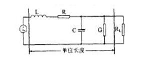
Figure 1 Equivalent circuit of unit length transmission line
According to Kirchhoff’s law, the transmission line equation can be expressed as
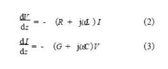
Therefore, the general solution of the transmission line equation can be written as

In the formula: V+, V-, I+, I- are the amplitude constants of the voltage wave and the current wave, respectively, and + and-respectively represent the transmission direction of the incident wave (+Z) and the reflected wave (-Z). The propagation constant C is defined as

In the formula: A is the attenuation constant; B is the phase constant. The voltage and current at a point on the transmission line are the superposition of the incident wave and the reflected wave, respectively. The voltage and current at any point on the Z axis are expressed as
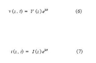
The above formula shows that the voltage wave and current wave transmitted on a transmission line are functions of time and transmission distance.
Integrated transmission line theory
Integrated transmission lines include microstrip lines, strip lines, coupled lines and various coplanar waveguides. Microstrip line is currently the most widely used planar transmission line in hybrid microwave integrated circuits and monolithic microwave integrated circuits. It can be used for lithography program production, and is easy to integrate with other passive microwave circuits and active microwave devices to realize the integration of microwave components and systems. The signal line of the microstrip line is on the outer layer, and the ground layer is on the other side of the signal line, which is easy to test.
The strip line, also known as the three-plate line, is composed of two rectangular cross-section conductor strips, and a uniform medium or air is filled between the grounding plates. The signal line of the stripline is sandwiched between two power layers. In theory, it can transmit the signal best because it is shielded by the power layer on both sides. But it hides the signal line inside and is not conducive to testing.
Signal integrity theory
Signal integrity (SI) mainly studies the quality and timing issues after the signal is transmitted along the wire. Generally, the signal integrity problems that need to be solved include: (1) reflection, caused by impedance mismatch; (2) crosstalk, caused by the coupling of adjacent signals; (3) overshoot and undershoot; (4) ringing, performance For the signal to oscillate repeatedly, it can be suppressed by proper termination; (5) Ground plane bounce noise and switching noise, for high-speed devices, a large number of data bus signals flip quickly, and the current change through the ground loop leads to a non-ideal ground plane; ( 6) Power distribution. For high-speed circuits, controlling the impedance of the power/ground plane is the key to system design; (7) Timing issues. For high-speed designs, signal propagation delay, clock offset, and jitter are enough to cause The system cannot correctly judge the data; (8) EMI problems include electromagnetic radiation and immunity. Solving EMI problems in PCB design is the most important link in system EMI control, and the cost is the lowest.
Simulation model and modeling method
SPICE simulation model and modeling method
SPICE simulation model SPICE (simulation program with integrated circuit emphasis) is a general circuit analysis program that can analyze and simulate various circuit characteristics under general conditions.
The SPICE program can replace the functions of the entire electronic laboratory such as breadboards and oscilloscopes. The SPICE program has a huge device library, including: (1) Passive device models, such as resistors, capacitors, inductors, transmission lines, etc.; (2) Semiconductor device models, such as diodes, transistors, junction field effect transistors, and MOS fields. Effect tube, etc.; (3) Various power supplies, including linear and non-linear controlled sources, such as independent voltage sources, current sources, controlled voltage sources, current sources, etc.; (4) A/D, D/A conversion interface Circuit and digital circuit device library.
The SPICE model modeling method usually uses two kinds of devices, one is discrete components and the other is chip. According to the type of device, two circuit modeling methods are adopted.
1) Basic device model. For example: resistors, capacitors, inductors, ordinary triodes, etc. These are the most basic units that make up a circuit. The physical method is usually used to model, that is, the model of the device is established with the equation describing the physical properties of the device as the starting point. The models of the same device under different operating frequencies are different.
2) Chip sub-circuit device model. Chips are usually composed of some basic components, and each basic unit component and its connection relationship are made into sub-circuits in the form of netlists, which can be called by other circuits to form a sub-circuit model of a chip. Usually black box (Blackbox) method is used to model, that is, the device is regarded as a black box, focusing on the working characteristics of the port, and using it to form a model.
IBIS simulation model and model structure
IBIS simulation model IBIS (input/output buffer information) input/output buffer information specification, is the standard model information of a component. The IBIS model is a method for quickly and accurately modeling I/O buffers based on the V/I curve. It is an international standard that reflects the electrical characteristics of chip driving and receiving. It provides a standard file format to record such as drives. Parameters such as output impedance, rise/fall time and output load are very suitable for calculation and simulation of high frequency effects such as ringing and crosstalk.
IBIS model structure IBIS model is a model used to describe the characteristics of I/O buffer information. The behavior description of an output and input port can be decomposed into a series of simple functional modules, and a complete IBIS model can be established from these simple functional modules., That is, the basic elements in a buffer unit, including the parasitic parameters (input, output or enable terminal) brought by the package, the parasitic capacitance of the silicon itself, the power or ground embedding protection circuit, the threshold and the enable logic, Pull-up and pull-down circuits, etc.
PCB simulation examples and results analysis
Setting of relevant parameters for PCB board simulation
There are two types of printed circuitboard simulation: line simulation and board level simulation. Line simulation can help designers adjust the layout of components, plan system clock networks and determine the termination strategy of key line networks before routing according to the requirements for signal integrity and timing during design, track the design during the routing process, and feedback the routing at any time Effect. Board-level simulation is usually carried out after the PCB design is basically completed. The influence of these factors on SI and the mutual influence of these factors such as electrical, EMC, thermal performance and mechanical performance can be comprehensively considered, so as to carry out real system-level analysis and verify. When performing simulation, first load the simulation model of the component, and then perform the pre-simulation to determine the parameter settings and some constraint conditions required in the wiring process. Then, check the wiring effect through line simulation at any time during the actual wiring process, and finally After the wiring is basically completed, board-level simulation is performed to check the performance of the system [6]. The example in this article is the reflection simulation analysis of SFP (small form-factor pluggable optical transceiver) small form-factor pluggable optical transceiver.
Simulation examples and result analysis
The simulation model is established after the schematic design of the SFP optical transceiver module is completed, the PCB board design should be started. Since the working frequency of the SFP optical transceiver module is set to 1.25Gbit/s, the data rate is very high, and the length of the differential trace is very long, so the impedance matching of the microstrip transmission line must be used to reduce the reflection at the source and terminal, thus Ensure the quality of the signal. According to the chip data of MAX3748 in the schematic diagram, the single-ended output impedance of the differential line is 50Ω, and according to the SFP-MSA protocol, the differential impedance of the RD+/- port on the motherboard is 100Ω. According to the theory of differential lines, in the absence of coupling, the differential impedance of two parallel microstrip transmission lines is equal to twice the single-ended impedance. Therefore, a transmission line with a characteristic impedance of 50Ω must be used for matching. Extract the topology of the interconnection network between MAX3748 and connector J1 as shown in Figure 2. Since J1 is a connector, there is no corresponding IBIS model data that can be called. Therefore, in order to make the simulation possible, load a differential receiver DIN1 that comes with the system at J1. And set the corresponding working frequency.
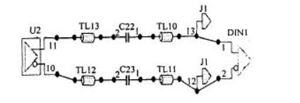
Figure 2 Topological structure of interconnection between MAX3748 and J1
Simulation results and analysis Through the analysis of simulation results, the signal quality does not meet the design requirements. The main problems are as follows: (1) Non-linearity in the rising and falling edges; (2) Certain overshoot and undershoot in the waveform; (3) ) The edge rate becomes slower. In view of the above problems, through further analysis of the circuit, it is found that these phenomena are caused by two factors. 1) Since the SFP optical transceiver module mainly uses differential lines for signal transmission, according to the SFP-MSA protocol, the differential impedance on the motherboard is 100Ω. Moreover, the impedance of the differential output end of the MAX3748 is 100Ω. In the previous simulation, when the system extracted the topology, the default impedance was 60Ω microstrip line, which caused impedance mismatch. 2) Since the differential input terminal of the system is loaded behind J1, when it is in the high impedance state, it is equivalent to the terminal open circuit situation, and there is a large reflection.
Therefore, in order to ensure the quality of the signal, impedance matching must be performed. Set the impedance of the differential transmission line to 100Ω. According to the theory of differential microstrip line, using transmission line calculation software can calculate the line width of the differential line to be 15mil, the line spacing is 10mil, and the corresponding single-ended impedance is about 62.5Ω. Since there is a certain coupling between the differential lines, the lossless microstrip line in the topological structure of the previous simulation is replaced with the actual lossy and coupled microstrip line for simulation analysis. At the same time, add a terminal resistance of 50Ω to the 3.3V power supply in the topology.
The modified topology is shown in Figure 3.
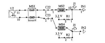
Figure 3 Modified topology
It can be known from the simulation waveform and eye diagram analysis that the signal has relatively good signal integrity. The overshoot amplitude of the signal is about 54mV, the rising and falling edges are about 100ps, and the swing amplitude of the differential output signal reaches about 850mV, which meets the signal output requirements.