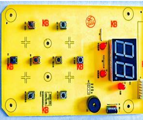
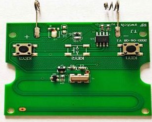
How to choose the correct solder mask for PCB circuit boards
The editor of PCB factory will introduce to you what is solder mask?
The solder mask is used to protect the metal elements on the PCB circuit board from oxidation, and if a small piece of solder adheres to the position where it should not be, a "bridge" is formed between the pads. If reflow soldering or soldering baths are used, this is a critical step in PCB manufacturing because these technologies do not have so much control to ensure that no solder joints are connected to where they should not be. Solder mask is sometimes called "solder resist", I think this is a better term because I used to think that solder mask is a whole layer of solder applied to the circuit board.

How to apply solder mask to PCB circuit board?
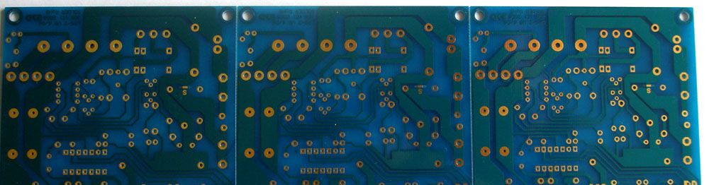
The solder mask contains a polymer layer that can be coated on the metal traces on the PCB circuit board. There are different types of mask materials, and the best choice for your PCB board depends on the cost and your application. The most basic solder mask option is to use screen printing to print liquid epoxy on the PCB. It's like spraying a topcoat with a stencil.
Fancier solder mask uses dry film or liquid solder mask for light imaging. Liquid photoimageable solder mask (LPSM) can be screen printed like epoxy or sprayed on the surface, which is usually a cheaper method of application. Dry film solder mask (DFSM) must be vacuum laminated to the circuit board to avoid bubble defects. Both optical imaging methods have been developed to remove the part of the mask that solders the pad to the component and cure it through a baking process or UV light exposure.
Solder mask is used as epoxy resin or photoimageable polymer.
Which solder mask should I use?
The determination of the appropriate solder mask depends on the physical dimensions of the circuit board, holes, components and conductors, surface layout and the final application of the product.
First of all, if you have a PCB solder mask, it will be used in aerospace, telecommunications, medical or other "high reliability" industries, check the industry standards of solder masks, and your general application. Some specific requirements supersede any other content you learn on the Internet.
For most modern printed circuit board designs, you need a photo-imageable solder resist. The surface topography will determine whether to use liquid or dry applications. Dry application spreads a uniform thickness on the entire surface. However, if the surface of your circuit board is very flat, the dry mask will adhere best. If you have complex surface features, then you may best use the liquid (LPISM) option for better contact with trace copper and laminate. The disadvantage of liquid applications is that the thickness of the entire plate is not completely uniform.
You can also obtain different finishes on the mask layer. Discuss with your PCB manufacturer what products are available to them and how it will affect production. For example, if a solder reflow process is used, a matte finish will reduce solder balls.
PCB manufactured using solder reflow process requires solder mask. The smoothness of the mask will affect the quality of reflow soldering.
How thick is my solder mask?
The thickness of your solder mask mainly depends on the thickness of the copper wire on the circuit board. Generally, you need about 0.5 mil solder mask on your trace. If a liquid mask is used, it must have a different thickness from other functions. In the empty laminate area, you can expect a thickness of 0.8-1.2 mils, while on complex features (such as the inflection point of a circuit), it may be as thin as 0.3 mils.
As with any other manufacturing parameters or process, you should consider the sensitivity of the final application and plan your design accordingly. It is always important to discuss manufacturing options with the manufacturer. They can even suggest better options based on their abilities.
How to add solder mask to the design?
When designing the printed circuit board, the solder mask should be its own layer in the Gerber file. Check the design rules of the solder mask. Generally, if the solder mask is not completely centered, you need to use a 2mil border around the function. The minimum distance between pads is usually 8 mils to ensure that the mask is sufficient to prevent solder bridges from forming.