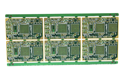
How big is the PCB circuit board design line width and line spacing rule setting
1. If the PCB circuit board design requires impedance signal lines, it should be set strictly according to the line width and line distance calculated by the stack. For example, radio frequency signals (conventional 50R control), important single-ended 50 ohms, differential 90 ohms, differential 100 ohms and other signal lines, the specific line width and line spacing can be calculated by stacking.
2. The line width and line spacing of PCB circuit board design should consider the production process capability of the selected multilayer PCB manufacturer. Necessary production costs, but the design can not be produced. Generally, the line width and line spacing are controlled to 6/6mil under normal circumstances, and the via hole is 12mil (0.3mm). Basically, more than 80% of PCB manufacturers can produce it, and the production cost is the lowest. The minimum line width and line spacing is controlled to 4/4mil, and the via hole is 8mil (0.2mm). Basically, more than 70% of multilayer PCB manufacturers can produce it, but the price is slightly more expensive than the first case, not too expensive. The minimum line width and line spacing are controlled to 3.5/3.5mil, and the via hole is 8mil (0.2mm). At this time, some multi-layer PCB manufacturers cannot produce it, and the price will be more expensive. The minimum line width and line spacing is controlled to 2/2mil, and the via hole is 4mil (0.1mm, at this time, it is generally HDI blind buried via design, and laser vias are required). At this time, most multilayer PCB manufacturers cannot produce it, and the price is The most expensive. The line width and line spacing here refer to the size between elements such as line-to-hole, line-to-line, line-to-pad, line-to-via, and hole-to-disk when setting rules.

3. Set rules to consider the design bottleneck in the design file. If there is a 1mm BGA chip, the pin depth is relatively shallow, only one signal line is needed between the two rows of pins, which can be set to 6/6 mil, the pin depth is deeper, and two rows of pins are required The signal line is set to 4/4mil; there is a 0.65mm BGA chip, which is generally set to 4/4mil; there is a 0.5mm BGA chip, the general line width and line spacing must be set to 3.5/3.5mil; there is a 0.4mm BGA Chips generally require HDI design. Generally, for the design bottleneck, you can set regional rules (see the end of the article for the setting method), set the local line width and line spacing to be smaller, and set the rules for other parts of the PCB to be larger, so as to facilitate production and improve the qualified rate of PCBs.
4. It needs to be set according to the density of the PCB circuit board design. The density is smaller and the circuit board is looser. The line width and line spacing can be set to be larger, and vice versa. The general can be set according to the following steps:
1) 8/8mil, 12mil (0.3mm) for via hole.
2) 6/6mil, 12mil (0.3mm) for via hole.
3) 4/4mil, 8mil (0.2mm) for via hole.
4) 3.5/3.5mil, 8mil (0.2mm) for via hole.
5) 3.5/3.5mil, 4mil (0.1mm, laser drilling) for via hole.
6) 2/2mil, 4mil (0.1mm, laser drilling) for via hole.