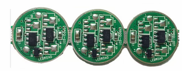
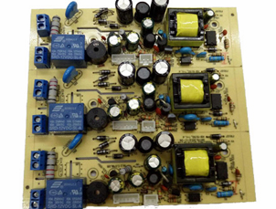
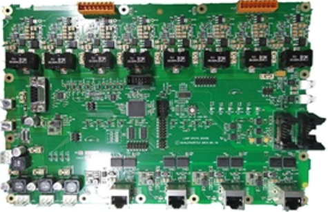
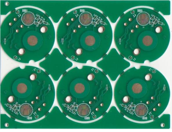
What problems should be paid attention to when using components for PCB proofing
In the proofing of PCB high-frequency boards, components with high sensitive voltage thresholds should be used as much as possible on the premise of meeting the functional requirements of the circuit. Because the electrostatic and discharge sensitivity of a circuit board depends on the component with the lowest sensitive voltage threshold in the circuit board.
1. Limit the output current to avoid the locking effect of CMOS circuit
The lock-in effect refers to the existence of parasitic PNP transistors and NPN transistors on the internal structure of the CMOS circuit, and a parasitic PNPN thyristor structure is formed between them. This kind of interlocking positive feedback structure may be triggered by external factors (such as electrostatic discharge), and current will flow on the PNP tube (or NPN tube), and then through another parasitic NPN tube (or PNP tube) to make the current Amplify, and due to the positive feedback, the current is getting larger and larger and eventually burned. It can be seen that limiting the current so that it cannot reach the level of maintaining the locked state is one of the issues to be considered for CMOS devices when PCB proofing.
The common solution is to use a resistor to isolate each output terminal from its cable, and use two high-speed switching diodes to clamp to VDD (drain power) and VSS (source power) with the cable. .

2. Use a filter network
Sometimes a long input cable is required between the CMOS circuit system and the mechanical contacts, which increases the possibility of electromagnetic interference, and a filter network should be considered. At the same time, long input lines are bound to be accompanied by larger distributed capacitances and distributed inductances, which can easily form LC self-excited oscillations, which will cause the diodes of the protection network to burn out. The solution is to connect a resistor in series at the input end, and its resistance can be selected according to the formula R=VDD/1mA.
3. RC network
Where feasible, for the sensitive input terminals of bipolar devices, an RC network composed of a resistor with a larger resistance value and a capacitor of at least 100pF can be used to reduce the impact of electrostatic discharge.
4. Avoid floating input pins of CMOS devices
In the PCB high-frequency board proofing, it is necessary to avoid the input end of the CMOS device soldered to the PCB circuit board from being left floating. At the same time, it should be noted that all unused redundant input leads on the CMOS device are not allowed to float. This is because once the input terminal is suspended, the input potential will be in an unstable state, which will not only destroy the normal logical relationship of the circuit, but also easily cause electrostatic breakdown and external noise interference. The redundant input terminal should be dealt with separately according to the function of the circuit.