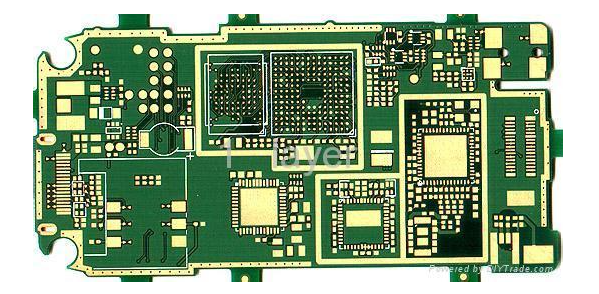
When the PCB circuit board proofing the plug-in component pad, the size of the pad should be appropriate. If the pad is too large, the spreading area of the solder will be larger, and the solder joint formed will not be full, while the surface tension of the copper foil of the smaller pad is too small, and the solder joint formed is a non-wetting solder joint. The matching gap between the aperture and the component line is too large, and it is easy to solder. When the aperture is 0.05~0.2mm wider than the lead and 2~2.5 times the diameter of the pad, it is an ideal condition for welding.
The purpose of PCB proofing in accordance with the requirements of the pad is to achieve the minimum diameter, which is at least 0.5mm larger than the maximum diameter of the small hole flange of the welding terminal. Test pads must be provided for all nodes in accordance with ANSI/IPC2221 requirements. A node is an electrical connection point between two or more components. A test pad requires a signal name (node signal name), the x-y coordinate axis related to the reference point of the printed circuit board, and the coordinate position of the test pad (indicating on which side of the printed circuit board the test pad is located).
PCB proofing considerations for the size of the pad aperture
The aspect ratio of the plated through holes has an important impact on the ability of the PCB proofing manufacturer to effectively electroplate the plated through holes, and it is also important in ensuring the reliability of the PTH/PTV structure. When the size of the hole is less than 1/4 of the thickness of the basic circuit board, the tolerance should be increased by 0.05mm. When the hole diameter is 0.35mm or less and the aspect ratio is 4:1 or greater, the PCB proofing manufacturer should use appropriate methods to cover or block the plated through holes to prevent solder from entering. Generally speaking, the ratio of the thickness of the printed circuit board to the pitch of the plated through holes should be less than 5:1. It is necessary to provide information on fixtures for SMT, as well as the warming technology of printed circuit board assembly layout, to promote the in-circuit with the help of "circuit test fixtures" or commonly referred to as "nail bed fixtures". Testability.

In order to achieve this goal, the following points need to be done:
1. Avoid plated through holes-probing on both sides of the printed circuit board. Put the test tip through the hole on the non-component/soldering surface of the printed circuit board. This approach can allow the use of reliable, less expensive devices. The number of different hole sizes should be kept to a minimum.
2. The diameter of the test pad dedicated for probing should not be less than 0.9mm.
3. Do not rely on the edge of the connector pointer for pad testing. The test probe can easily damage the gold-plated pointer.
4. The space around the test pad should be greater than 0.6mm and less than 5mm. If the height of the component is greater than 6.7mm, the test pad should be placed 5mm away from the component.
5. Do not place any components or test pads within 3mm from the edge of the printed circuit board.
6. The test pad should be placed in the center of a 2.5mm hole in a grid. If possible, allow the use of standard probes and a more reliable fixture.