Wit the development of electronic products with high density and high precision, the same requirements are put forward relative to the auxiliary circuit board, and the circuit board gradually develops in the direction of HDI. The most effective way to increase the density of PCB is to reduce the number of through holes, and to set blind holes and buried holes very accurately.
1. Blind hole definition
a: In contrast to through holes, through holes refer to holes drilled through all layers, while blind holes are through holes drilled straight and straight.
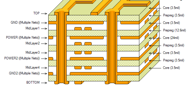
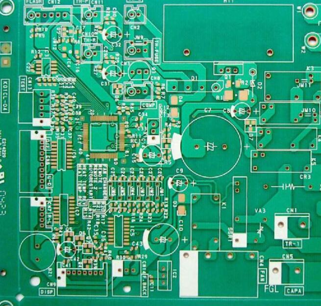
(The graphic explanation is clear, an example of an eight-layer board: through hole, blind hole, buried hole)
b: Blind hole subdivision:
Blind hole (BLIND HOLE), buried hole BURIED HOLE (outer layer can not be seen);
c: Different from the manufacturing process:
Blind holes are drilled before pressing, while through holes are drilled after pressing.
2. Manufacturing method:
a: Drill belt:
(1): Select reference point: Select the through hole (ie a hole in the first drilled belt) as the unit reference hole.
(2): Each blind hole drilling belt needs to select a hole to indicate the coordinates of the relative unit reference hole.
(3): Pay attention to explain which drill belt corresponds to which layers:
The unit sub-hole diagram and the drill table must be marked, and the names of the front and back must be exactly the same; it cannot be revealed that the sub-hole diagram is expressed in a b c, and the situation in front of it is expressed in 1st and 2nd.
Note that when the laser hole and the inner buried hole are sleeved together, that is, the holes of the two drill belts are in the same position, you need to ask the customer to move the position of the laser hole to ensure the electrical connection.

B: Produced pnl board edge process hole: ordinary multi-layer board: the inner layer is not drilled;
(1): Rivet gh, aoi gh, et gh are all played after the board is eroded (beer out)
(2): target hole (drilling gh) ccd:
The outer layer needs to take out the copper skin, x-ray machine:
Type directly, and note that the minimum length of the long side is 11 inches.
HDI blind hole plate:
All tooling holes are drilled, pay attention to the rivet gh; need to be brewed to prevent misalignment.
(aoi gh is also for beer), the edge of the pnl board must be drilled to distinguish each board.
3. Film correction:
(1): Indicate that the film has a positive film, and a negative film:
General principles:
If the board thickness is greater than 8mil (without copper), take the positive film process;
The thickness of the board is less than 8mil (without copper) and the negative film process (thin board);
When the line thickness is large, the copper thickness at d/f needs to be considered, not the bottom copper thickness.
The blind hole ring can be made 5mil, no need to make 7mil.
The inner independent pad corresponding to the blind hole needs to be saved.
Blind holes cannot be made without ring holes.
4. Process: The buried-hole plate is exactly the same as the usual double-sided board.
HDI blind hole plate, that is, one side is the outer layer:
Positive film process: single-sided d/f is required, and you must not roll the wrong side (when the copper on both sides is not exactly the same); when d/f is exposed, the polished copper surface is covered with black tape to avoid light transmission.
Because the blind hole board is made more than two times, the thickness of the finished product is very easy to be too thick, because the thickness of the board should be controlled in this map, and the range of the copper thickness should be indicated after the etching.
After pressing the board, use the x-ray machine to punch out the target holes for the multilayer board.
Negative film process: For thin plates (<12mil with="" copper="">) because it cannot be produced in the drawing circuit, it must be produced in the hydro-metal drawing, and the hydro-metal drawing cannot be divided into currents, so there is no way to do single-sided non-printing according to the mi requirements Electric current or small current.
If the positive film process is used, the copper thickness on one side is often too thick, which leads to the phenomenon of difficult etching and thin lines, because this type of board requires a negative film process.
5. Through holes and blind holes are drilled in different order, and the deviations during manufacturing are not exactly the same; blind hole plates are more prone to deform and deform, and it is difficult to control the alignment of the multilayer board and the tube pitch when the horizontal and vertical materials are opened. When opening the material, only the horizontal material or only the straight material is opened.
6. Laser drill:
LASER DRILL is a kind of blind hole and has its own unique place:
Aperture volume:
4-6 mil pp thickness shall be <=4.5mil, calculated based on aspect ratio<=0.75:1
There are three types of pp: LDPP 106 1080; FR4 106 1080; RCC.
7. How to define the need for natural resin plug holes for buried-hole plates:
a. H1 (CCL): H2 (PP) 〉=4 thickness ratio
b. HI (CCL) 》32 MIL c.2OZ and above 2OZ laser buried hole plate;
High-thickness copper and high-tg boardsneed to be sealed with natural resin as deemed appropriate.
In the boarding process of this type of board, attention should be paid to sealing the holes with natural resin before making the circuit so as not to cause greater damage to the circuit.