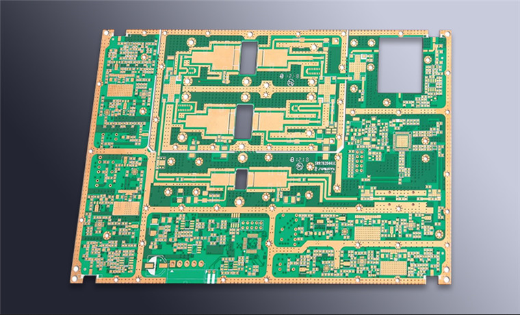
Multilayer circuit board factory: the difference between positive and negative
PCB factory:Multilayer circuit board negative film: generally we talk about the tenting process, the chemical solution used is acid etching negative film because after the film is made, the required circuit or copper surface is transparent, and the unneeded part is It is black. After the circuit process is exposed, the transparent part is chemically cured by the dry film resist being exposed to light. The subsequent development process will wash off the uncured dry film, so only the dry film will be etched during the etching process. The copper foil of the film is washed away (the black part of the negative film), and the dry film is not washed off, which belongs to the circuit we want (the transparent part of the negative film)
Multilayer circuit board positive film: generally we talk about the pattern process, the yao liquid used is alkaline etching positive film. If you look at the negative film, the required circuit or copper surface is black, and the other part is transparent In the same way, after exposure through the circuit process, the transparent part is chemically hardened by the dry film resist being exposed to light. Lead is plated on the copper surface washed away by the dry film in the previous process (development), and then the film is removed (removing the dry film hardened by light). Drop the copper foil without tin-lead protection (the transparent part of the negative), and the rest is the circuit we want (the black part of the negative)
Positive film and negative film are actually selected according to the process of each circuit board factory. Positive film: The process is (double-sided circuit board) cutting-drilling-PTH (one-time plating is also called thickened copper)-circuit-two copper (graphic plating) ) Then take the SES line (removal film-etching-stripping tin) negative film: the process is (double-sided) cutting-drilling-PTH (one-time plating is also called thickened copper)-line (without two copper pattern plating) and then go DES line (etching-removing film)

1. Distinguish between the master film (negative film), the working film, the positive and negative film and the film surface: the film has the master film and the working film (child film), black film and yellow film, positive film and negative film;
2. Pay attention to the use of yellow film: there are two kinds of glossy surface and matte surface. The second type is prone to oil surface indentation when used;
3. When distinguishing the yao film surface, the black and smooth surface is the medicated film, while the yellow film is the opposite. Generally, you can see that the side is the medicated surface by scraping the film with a scraper or a blade. (Master film: orthographic positive medicine surface, sub-film: orthographic negative medicine surface);
4. Generally speaking, the master film is black film, also known as silver salt film, which is mainly used to copy the work film (yellow film is also called diazo film), but the work film is not necessarily only the yellow film. There are also black films as the work film. It is used in the production of high-precision HDI boards or in the production of one-off small-batch circuit boards in order to save costs. Yellow films are used in the manufacture of ordinary PCB circuit boards and mass-produced ordinary circuit boards;
5. The light-transmitting negative film on the film circuit (with copper), the opaque film is the positive film; the positive film is used for pattern electroplating, the circuit is developed, and the remaining function is anti-corrosion electroplating, which is mainly plated with lead and tin . The negative film is used for direct etching, and the resist left after development is a circuit, which is directly etched with an acid etching solution.