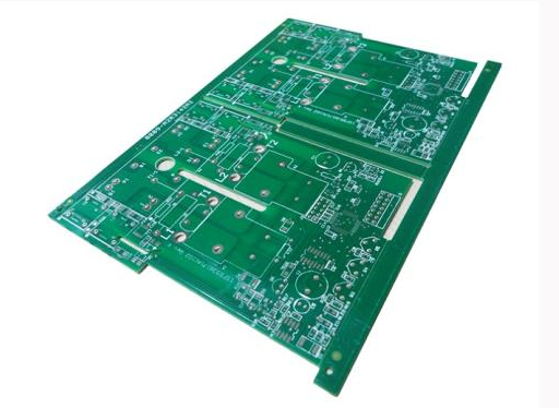
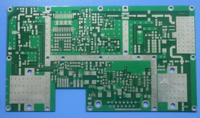
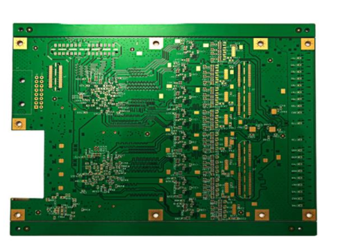
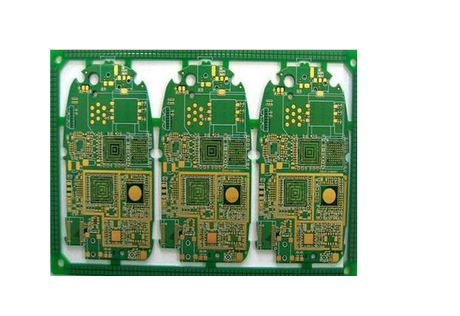
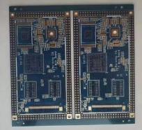
Introduction of the fine line of multi-layer circuit board
With the rapid development of electronic information technology, all fields of communications, medical care, industrial control, storage services, aerospace, and personal consumption have also entered the era of great development. Upstream and downstream companies in the electronics industry are constantly striving to improve their technical capabilities to respond to customers in various fields. The demand for the benefit of the increase. As electronic products continue to develop towards miniaturization, high-density, and high-speed development, the requirements for multilayer PCB products are becoming increasingly strict.
1. The development trend of fine lines
Multi-layer PCB products have different uses and different levels of demand for fine lines. Aviation, medical and other products pursue high reliability, with thick copper, wide lines, and large pads. The general line design is above 4mil, and consumer products pursue high reliability. The functions are complex and diverse, and the reliability requirements are not high. The copper thickness is thin and the circuit is fine. The general circuit design is between 0.05mm and 0.075mm. The number of layers of this circuit is generally high-density multi-layer circuit boards, while communication products are Somewhere in between. Package carrier products are carriers of IC components, and their line density needs to meet the needs of IC packaging, and the line density requirements range from a few microns to tens of microns.
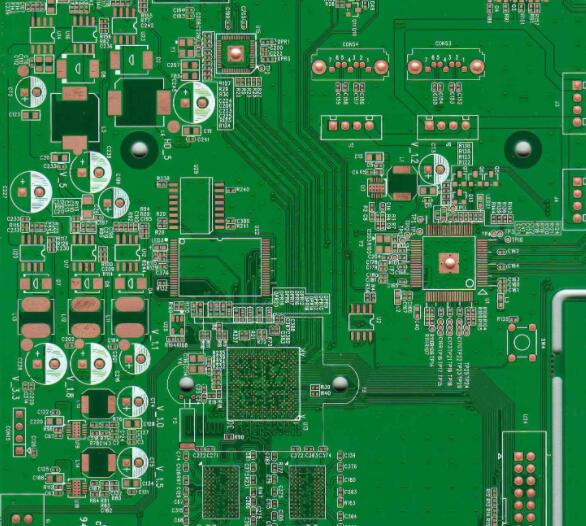
2. Factors influencing the processing of fine lines on Multilayer circuit board (graphic production)
Graphic production technology, including resist film adhesion, exposure machine.
Resist film selection: There are two main processes for the production of inner layer patterns: dry film and wet film. The thickness of the wet film is thin, the exposure time is short, and the resolution of 0.05mm/0.05mm can be achieved, but it is highly affected by the environment and operation. Scratches and small dust can cause the gap to open. At the same time, the wet film coating and baking time are long, which is not suitable for sample processing. Compared with the wet film, the dry film has a thicker thickness, but has better uniformity and stable quality. It can also meet the resolution of 0.05mm/0.05mm. At present, most factories use wet film to process large quantities of thick line products, and dry film processing is mostly used for fine lines.
3. Factors influencing the processing of fine lines on multilayer circuit boards (graphic exposure)
Graphic Exposure: Exposure is the key to affecting graphic capabilities, which is related to the clean room environment, the type of exposure machine, and the operating skills of the staff. Exposure machines are divided into parallel light and scattered light according to the type of light source. The parallel light has uniform energy distribution and high resolution, but the use cost is also high. In order to ensure the processing capacity of fine lines, a parallel light exposure machine is required. According to the operation mode, it is divided into manual, semi-automatic and automatic. The automatic exposure machine has high alignment accuracy, strong vacuuming ability, low film cleaning frequency, and low operation requirements for employees. In order to ensure the product yield and ability, the automatic exposure machine should be used. .

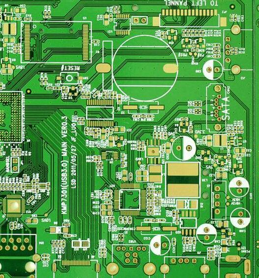
4. Factors influencing the processing of fine-grained multilayer circuit boards (plating technology)
The thickness of the copper to be etched is a key factor affecting the processing capability of fine lines, and the electroplating ability often determines the thickness of the copper to be etched. Electroplating ability mainly includes deep plating ability and copper thickness uniformity. At present, electroplating equipment in the industry is mainly divided into vertical electroplating (longmen electroplating), vertical continuous electroplating (VCP) and horizontal electroplating according to electroplating methods. Among them, the vertical electroplating ability is good, and the VCP horizontal electroplating uniformity is good. Therefore, in order to make the quality of fine and dense circuit boards more stable, it is best to use VCP level electroplating equipment.
5. Factors influencing the processing of fine lines on multilayer circuit boards (etching technology)
Process method: The etching process is mainly divided into subtractive method, semi-additive method and full-additive method. Among them, masking process (subtractive method) and electrical drawing process (a kind of semi-additive method) are mainly used in ordinary PCB processing. ), compared with the masking process, the copper thickness required to be etched in the patterning process is thinner, but the patterning process is affected by the pattern distribution, and some products have poor electroplating uniformity and a longer process. Cost and efficiency improvement are generally based on the masking process.
This limited company is a professional manufacturer of high-precision PCB multilayer circuit boards.