Multilayer circuit board manufacturers
PCB double-sided printed circuit board manufacturing process In recent years, the typical process for manufacturing double-faced metalized printed circuit boards is the SMOBC method and the pattern plating method. In some specific occasions, the process wire method is also used.
1., graphic electroplating process
Foil-clad laminate-blanking-punching and drilling of benchmark holes-CNC drilling-inspection-deburring-electroless thin copper plating-electroplating thin copper-inspection-brushing-filming (or screen printing )-Exposure and development (or curing)-inspection and repair-pattern plating (Cn + Sn/Pb)-film removal-etching-inspection and AS repair-plug nickel plating and gold plating-hot melt cleaning- Electrical continuity inspection-cleaning treatment-screen printing solder mask graphics-curing-screen printing marking symbols-curing-shape processing-cleaning and drying-inspection-packaging-finished circuit board.
In the process, the two processes of "electroless plating of thin copper -> electroplating of thin copper" can be replaced by one process of "electroless plating of thick copper", both of which have their own advantages and disadvantages. Pattern electroplating---etching method to make double-faced metallized plates is a typical process in the 1960s and 1970s. The bare copper-clad solder mask process (SMOBC) gradually developed in the mid-1980s, and has become the mainstream process especially in the manufacture of precision double-sided PCB boards.
, why should the BGA of the multilayer circuit board be in the solder mask hole? What is its reception standard?
Answer: First of all, the solder mask hole of the multilayer circuit board is to protect the service life of the via, because the hole required to plug the BGA position in the multilayer circuit board is generally relatively small, between 0.2~0.35mm. During the post-process processing, some of the syrup in the hole is not easy to be dried or evaporated, and it is easy to leave residues. If the hole is not plugged in the solder mask or the plug is not full, the subsequent processing such as tin spraying and gold immersion will be there. Residual foreign matter or tin beads. When the customer installs the component and is heated at high temperature, the foreign matter or tin beads in the hole will flow out and adhere to the component. The circuit board manufacturer will cause the component performance defect, such as: open, short circuit . The BGA is located in the solder mask hole A, must be full B, no redness or false copper exposure is allowed, C, no too full, and the protrusion is higher than the pad to be soldered next to it (which will affect the component mounting Effect). Circuit board

Iii, what is side development? What are the quality consequences caused by side development?
The bottom width area of the part where the green oil on one side of the solder mask window has been developed is called side development. When the side development is too large, it means that the green oil area of the part that is developed and which is in contact with the substrate or copper skin is larger, and the degree of dangling formed by it is larger. The subsequent processing such as tin spraying, tin sinking, Immersion gold and other side developing parts are attacked by high temperature, pressure and some potions that are more aggressive to green oil. Oil will drop. If there is a green oil bridge on the IC position, it will be caused when the customer installs the welding components. Will cause a bridge short circuit. Circuit board
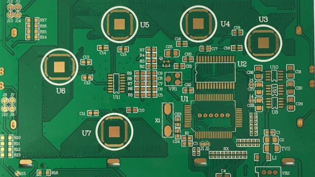
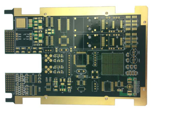
What are the holes on the multilayer circuit board?
To be precise, this cannot be called a hole. The technical term is called a hole. The holes on the circuit board (PCB) are divided into three types: via holes (VIA), plug-in holes, and mounting holes. Via holes play the role of conduction and heat dissipation; plug-in holes are used for welding components, and the corners of the components are inserted and fixed with tin; mounting holes are used for screwing, and can be assembled with other components. Circuit board
Generally speaking, via holes and plug-in holes are metallized holes (PTH), that is, the hole walls are metal attached and can conduct electricity, and the mounting holes are generally non-metallized holes (NPTH), and the hole wall is the substrate.
This hole is drilled by a CNC drilling machine or laser, and then undergoes chemical copper plating, copper electroplating, and surface treatment (commonly sprayed tin and gold, and others have anti-oxidation, tin sink, etc.).
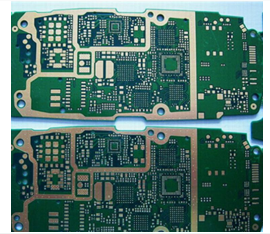
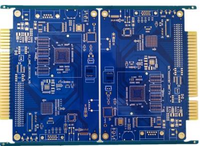
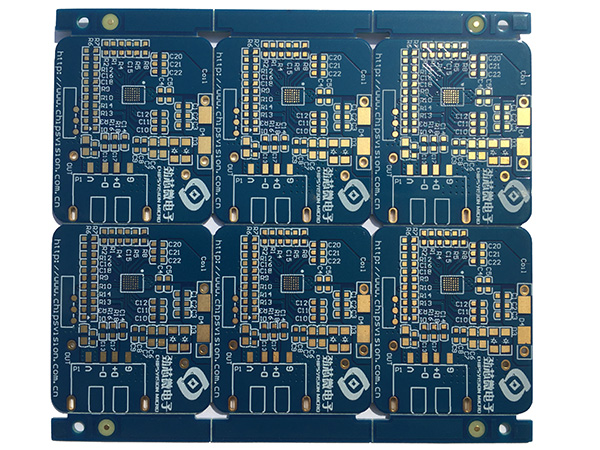
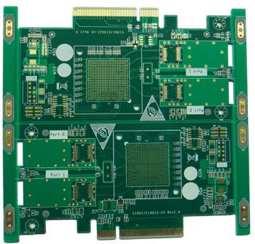
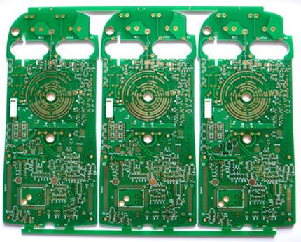
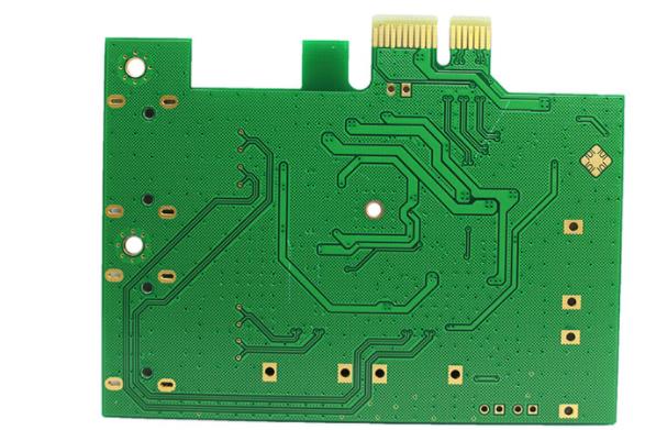
Generally, the multi-layer circuit boards we see come in various colors, which are called solder masks, which prevent short circuits and protect the board, which plays a beautiful role. Characters will be printed on the solder mask to facilitate identification of components during soldering repairs. The inks are green, white, red, yellow, blue, black, etc.
PCB multi-layer circuit board design welding design specification
⑴, Whether there is a 3mm wide reserved bracket position in the middle of the PCB board that is wider than 180mm or longer than 320mm for wave soldering. Circuit board
⑵, the direction of wave soldering should be clearly marked on the upper and lower sides of the circuit board.
(3) The reserved position of the support bar should not be within the bending range of the component lead.
⑷, try not to lay out the components like horizontal plug-in wires and other spatial dimensions protruding from the edge of the board.
⑸, the bend of the lead of the electrical plug component, the area around the triode, IC and the socket pin pads, should be coated with a secondary solder mask.
⑹, due to structural limitations, components that are not suitable for wave soldering, it is necessary to add a tin bath at the position opposite to the direction of the wave crest, and the groove width is 0.7 mm.
⑺, a large area of copper foil is easy to be heated to produce copper foil expansion, so the area exceeds the diameter of the 15mm circle, the conductive layer needs to open a conductive window or grid.