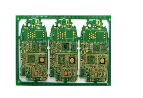
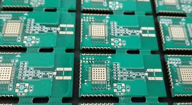
Multilayer PCB design principles
Multilayer PCB boards are usually used in high-speed, high-performance systems, some of which are used for power or ground reference planes, and these planes are usually solid planes without partitions. Regardless of the purpose of these layers and the voltage, they will serve as current return paths for adjacent signal traces. The most important thing to construct a good low-impedance current return path is to plan the design of these reference planes reasonably. Shown is a typical multilayer PCB stack configuration.
The signal layer is mostly located between these metal solid reference plane layers, forming a symmetrical stripline or an asymmetrical stripline. In addition, the upper and lower surfaces (top and bottom) of the board are mainly used to place component pads. There are also some signal traces on them, but they should not be too long to reduce direct radiation from the traces.
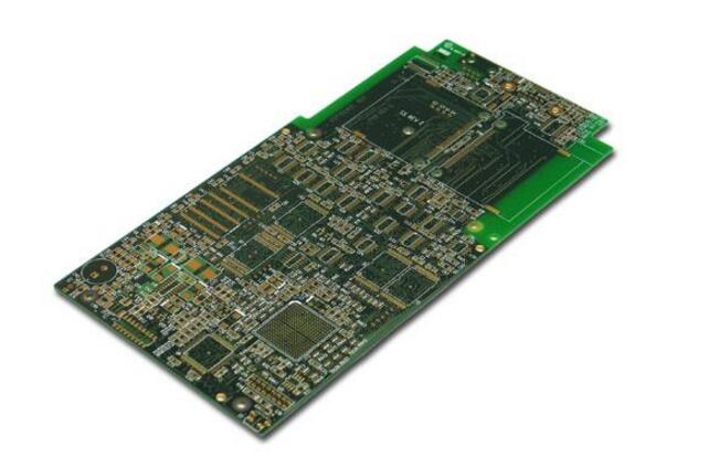
P is usually used to represent the reference plane layer; S represents the signal layer; T represents the top layer; B represents the bottom layer. Below is a 12-layer PCB circuit board to illustrate the structure and layout of the multilayer PCB board, as shown in Figure 6-14. -S-s-P-B". The following are some principles for multilayer PCB design.

1. Set the DC voltage for the reference plane: An important measure to solve the power integrity is to use decoupling capacitors. The decoupling capacitors can only be placed on the top and bottom layers of the PCB. The effect of the decoupling capacitors will be severely affected by the connection The influence of lines, pads, and vias requires that the traces connecting the decoupling capacitors be as short and wide as possible, and the vias are as short as possible. As shown in the figure, the second layer is set as the power supply for high-speed digital devices (such as processors); the fourth layer is set as the high-speed digital ground; and the decoupling power supply is placed on the top layer of the PCB circuit board; this is a kind of More reasonable design. In addition, try to ensure that the signal traces driven by the same high-speed device use the same power layer as the reference plane, and this power layer is the power source of the high-speed device.
2. Determine the multi-power reference plane: the multi-power layer will be divided into several physical areas with different voltages. As shown in the figure, the 11th layer is allocated as the multi-power layer, then the nearby 10th layer and the signal on the bottom layer The current will encounter an undesirable return path, causing gaps in the return path. For high-speed signals, this unreasonable return path design may cause serious problems. Therefore, high-speed signal wiring should be far away from the multi-power reference plane.
3. Multiple ground copper layers can effectively reduce the impedance of the PCB circuit board and reduce common mode EMI.
4. The signal layer should be tightly coupled with the adjacent reference plane (that is, the dielectric thickness between the signal layer and the adjacent copper layer should be small); the power copper and ground copper should be tightly coupled.
5. Reasonably design the wiring combination: In order to complete the complex wiring, the layer-to-layer conversion of the multi-layer PCB board wiring is inevitable, and the two layers spanned by the same signal path are called a "wiring combination". When switching between signal layers, it is necessary to ensure that the return current can flow smoothly from one reference plane to another reference plane. In fact, the most common wiring combination design is to avoid the return current from flowing from one reference plane to another, but to simply flow from one surface of the reference plane to another. As shown in the figure, the 3rd and 5th layers, the 5th and 7th layers, and the 7th and 9th layers can all be used as a wiring combination. However, it is not a reasonable design to use the 3rd and 9th layers as a wiring combination. It requires the return current to be coupled from the 4th layer to the 6th layer, and then from the 6th layer to the 8th layer. This path is for the return current It is not smooth. Although it is possible to reduce ground bounce by placing decoupling capacitors near the vias or reducing the thickness of the dielectric between the reference planes, it is not a best strategy and may not be implemented in actual systems.
6. Set the wiring direction: On the same signal layer, ensure that most of the wiring directions are consistent and orthogonal to the wiring direction of adjacent signal layers. As shown in the figure, the wiring directions of the 3rd and 7th layers can be set as the "north-south" direction, and the wiring directions of the 5th and 9th layers can be set as the "east-west" direction.
iPCB is a high-tech manufacturing enterprise focusing on the development and production of high-precision PCBs. iPCB is happy to be your business partner. Our business goal is to become the most professional prototyping PCB manufacturer in the world. Mainly focus on microwave high frequency PCB, high frequency mixed pressure, ultra-high multi-layer IC testing, from 1+ to 6+ HDI, Anylayer HDI, IC Substrate, IC test board, rigid flexible PCB, ordinary multi-layer FR4 PCB, etc. Products are widely used in industry 4.0, communications, industrial control, digital, power, computers, automobiles, medical, aerospace, instrumentation, Internet of Things and other fields.