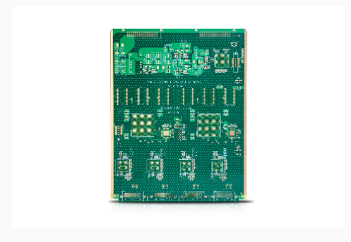
Multi-layer circuit board production needs to be considered
At present, in the field of electronic product processing, multilayer circuit boards are indispensable as one of the important electronic components. At present, there are many types of PCB circuit boards, such as high-frequency circuit board plates, microwave circuit boards and other types of printed circuit boards that have gained a certain reputation in the market. Multilayer circuit board factories have specific processing techniques for various board types. But in general, multilayer circuit board manufacturers need to consider three major aspects.
1. Consider the choice of process flow
The production of multi-layer circuit boards is easily affected by many factors, and the number of processing layers, perforation technology, surface coating treatment and other processes will affect the quality of the finished PCB circuit board. Therefore, for these process environments, multilayer circuit board production is fully considered in combination with the characteristics of the production equipment, and can be flexibly adjusted according to the types of PCB boards and processing requirements.

2. Consider the choice of substrate
The base material of the circuit board can be divided into two types: organic material and inorganic material, each material has its own unique advantages. Therefore, the determination of the type of substrate considers various properties such as dielectric properties, copper foil type, base groove thickness, and processability characteristics. Among them, the thickness of the surface copper foil is a key factor affecting the performance of this printed circuit board. Generally speaking, the thinner the thickness, the more convenient the etching and the improvement of the precision of the graphics.
3. Consider the setting of the production environment
The environment of the multi-layer circuit board manufacturing workshop is also a very important aspect. The regulation of the ambient temperature and the ambient humidity are both crucial factors. If the ambient temperature changes too significantly, it may cause the holes on the base plate to break. If the environmental humidity is too high, nuclear energy will have an adverse effect on the performance of the substrate with strong water absorption, specifically in terms of dielectric properties. Therefore, it is very necessary for circuit board manufacturers to maintain proper environmental conditions during production.
What problems are prone to occur in the process of PCB plate making
When we design on the PCB design software, it is often because of the seemingly connected parts (electrical performance) on the plane that are not actually connected. Therefore, when we start to make a plate based on the design file, the sequential operation is very important . Today we use the following three methods to focus on solving the problems that are prone to occur in the process of PCB plate making.
1. Make a physical border
Making a closed physical frame on the original board is a constraint on the layout and wiring of the later components. Through the setting of a reasonable physical frame, the welding of the components and the accuracy of the wiring can be more standardized. But pay special attention to the fact that the physical borders of some curved edge boards or corners should also be set in an arc shape. The first is to prevent sharp corners from scratching workers, and the second is to reduce stress to ensure safety during transportation.
2. The introduction of components and networks
It should be very simple to draw the components and the network in the frame, but there are often problems here. You must carefully solve the errors one by one according to the prompts. Otherwise, it will take more effort. The problems here generally include the following:
The package form of the component can not be found, the component network problem, there are unused components or pins, these problems can be solved quickly by comparison.
3. Layout standardization of components
(1) Placement order
Experienced installers will first place the components in fixed positions related to the structure, such as power sockets, indicator lights, switches, connectors, etc. Then lock it through the software to ensure that the fixed position of the components will move or affect when other components are placed later. For complex boards, we can divide them into the order of placement and operate them several times.
(2) Pay attention to the influence of layout on heat dissipation
The component layout should pay special attention to heat dissipation. For high-power circuits, the heating elements such as power tubes, transformers, etc. should be placed as close to the side as possible to facilitate heat dissipation. Do not concentrate in one place, and do not have high capacitors too close to avoid premature aging of the electrolyte.
ipcb is a high-precision, high-quality PCB manufacturer, such as: isola 370hr PCB, high-frequency PCB, high-speed PCB, ic substrate, ic test board, impedance PCB, HDI PCB, Rigid-Flex PCB, buried blind PCB, advanced PCB, microwave PCB, telfon PCB and other ipcb are good at PCB manufacturing.