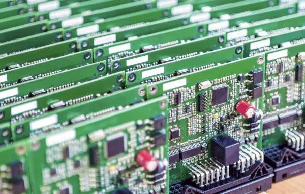
If you want to make your own smart audio HDI factory layout, then getting ready may just help organize and remember important design details. However, if the design is sent to others for layout, lack of preparation in this regard may cause a lot of trouble to complete the design.
Let's take a look at what things should be considered in the schematic to make it easier to convert the PCB layout.
How to convert PCB layout? The first rule: clean documentation
The circuit design may come from scribbled notes on paper, or schematic diagrams drawn hastily on the blackboard, but these are certainly not the correct way to document. At present, many medical institutions are forcing doctors to use electronic files instead of pen and paper to record prescriptions. This is to make it easier for patients to read them.
Just as it is important to be able to read the prescription correctly, so is the detailed information and instructions in the schematic. Do yourself a favor and take a moment to make sure the schematic is clear and easy to read.
Here are some tips on how to do it correctly:
Use grid alignment symbols to draw straight lines and organize text.
The font and line width of the text used should be large enough to be easy to read, but not too large to avoid confusing the schematic.
Don't crowd symbols and text together, leave some space for them so that you can read them accurately.
Write a schematic diagram with a meaningful logical flow. There is no need to get components stuck in a certain area, as long as they do not belong to that area, they can be blocked.
If you can create a more readable document, you don't have to worry about using other pages in the schematic.
If you give yourself enough time to create easy-to-use documents, you will get the convenience of a lot of extra effort during the layout process.

Library parts are essential for converting PCB layout
Another important part of successfully converting a schematic into a PCB layout is to ensure that the library parts are current and correct. The part represented by the symbol must be correct. This includes pushpins, text, shapes and attributes. Sometimes people use existing symbols as templates to build new symbols, and then ignore adding, deleting, or modifying parts of the original message. The better situation is that when the part number on the schematic drawing does not match the part number reported in the report, it may cause a lot of confusion. The worst case is that the symbolic information is completely wrong and causes connection errors in the schematic or downstream tools (such as simulators).
When building a new symbol for your design, make sure to also include all relevant component information. This will include the physical footprint name of the layout tool, company part number, supplier part number, cost information and simulation data. Every company has its own standards for what should or should not be included in the library section, but it is better to have too much information than to have less. When you are done, make sure to populate the new parts into the appropriate component library, and make sure that the parts on the schematic have also been updated to reference the correct library.

Detailed and complete schematic information is very important
Just as there is not much information in the library parts, this also applies to schematics. You need to be careful not to add too much data to make the schematic difficult to read, but you should add enough complete information to help downstream personnel in the layout, testing and rework. Here are some examples of related information:
Schematic diagram of the identification of the functional area ("power supply", "fan control", etc.).
Test the location of power, ground or specific signals.
Layout placement of fixed components (such as connectors and plugs).
The components are grouped to identify high-speed or sensitive placement areas.
Sensitive circuits that may require special attention, such as RF shielding.
Hot areas of concern.
High-speed PCB requirements, such as measured trace length or controlled impedance routing.
Differential pair.
In addition to the functional information listed above, don't forget to include all regular schematic document data. This will include items in the title bar, such as company name, part number, revision, board name, date and copyright information. By ensuring that there is enough complete information on the schematic, and as much data as possible, but not too cumbersome, it will help to ensure that the schematic is successfully converted into a PCB circuit board layout.