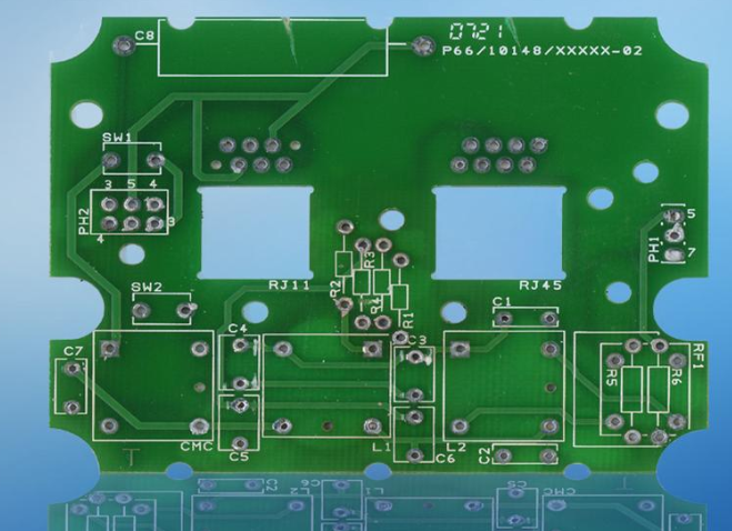
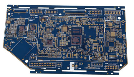
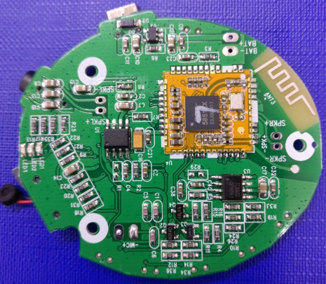
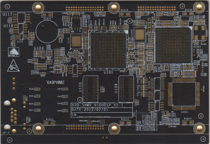
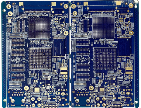
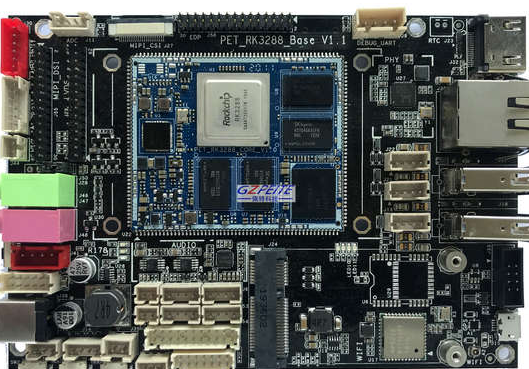
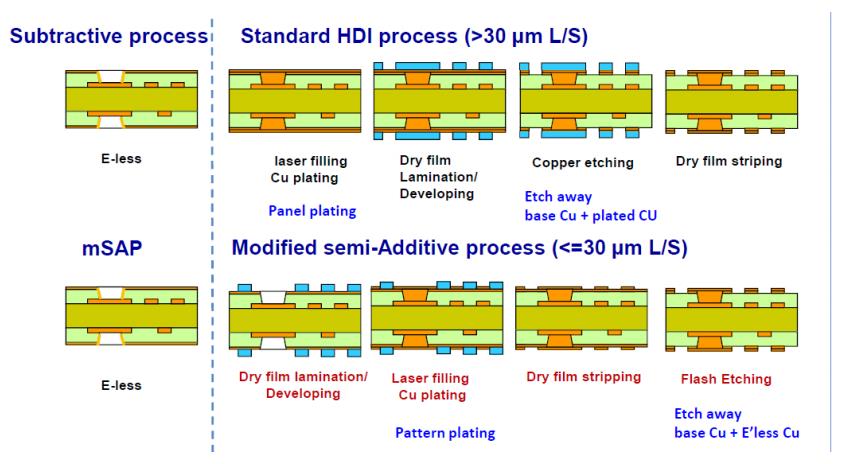
Overview of HDI high-density technology for printed circuit boards, application of HDI circuit board production technology

(1) Fine wire technology In the future, the high and fine wire width/spacing will be 0.20mm-O.13mm-0.08mm-0.05mm to meet the requirements of SMT patch, Multichip Package and MCP. Therefore, the following technology is required.
1. Because the line width of HDI circuit board is very thin, thin or ultra-thin copper foil (<18um) substrate and fine surface treatment technology are now used.
2. The current HDI circuit board production has adopted thinner dry film and wet filming processes. The thin and good quality dry film can reduce line width distortion and defects. Wet film can fill small air gaps, increase interface adhesion, and improve wire integrity and accuracy.
3. HDI circuit board circuit etching adopts electro-deposited photoresist (Electro-deposited Photoresist, ED). Its thickness can be controlled in the range of 5-30/um, which can produce more perfect fine wires. It is especially suitable for narrow ring width, no ring width and full plate electroplating. There are currently more than a dozen ED production lines in the world.
4. HDI circuit board circuit imaging adopts parallel light exposure technology. Since parallel light exposure can overcome the influence of the line width variation caused by the oblique rays of the "point" light source, it is possible to obtain fine wires with precise line width dimensions and smooth edges. However, the parallel exposure equipment is expensive, the investment is high, and it is required to work in a high cleanliness environment.
5. HDI circuit board inspection adopts automatic optical inspection technology (Automatic Optic Inspection, AOI). This technology has become an indispensable means of detection in the production of fine wires, and is rapidly being promoted, applied and developed. For example, AT&T company has 11 AoIs, while tADCo has 21 AoIs dedicated to detecting inner-layer graphics.