What points should be paid attention to in the PCB design of the DC-DC of the PCB factory?
The circuit of IaDC-DC is much more complicated than LDO, and the noise is higher. PCB manufacturers have higher requirements on layout and layout. The quality of the layout directly affects the performance of DC-DC, so it is very important to understand the layout of DC-DC.
1. Bad layout
EMI, DC-DC SW pin will have higher dv/dt, higher dv/dt will cause larger EMI interference;
Ground noise, poor ground wiring, will produce relatively large switching noise on the ground wire, and these noises will affect other parts of the circuit;
The PCB factory produces voltage drop on the wiring, and if the wiring is too long, it will cause a voltage drop on the wiring and reduce the efficiency of the entire DC-DC;
2. General principles
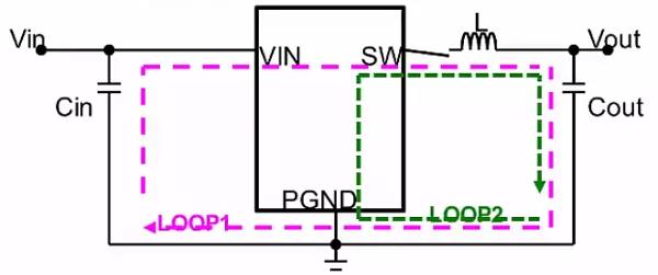
The switch high current loop should be as short as possible;
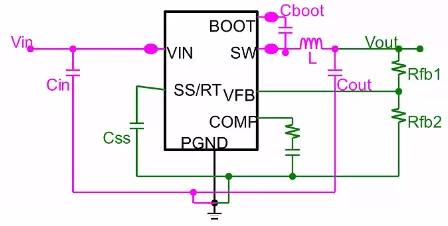
Signal ground and high current ground (power ground) are routed separately and connected at a single point at the chip GND;
1. The switching circuit is short. The red LOOP1 in the figure below indicates that the DC-DC high-side tube is turned on, and the current flow direction when the low-side tube is turned off; the green LOOP2 is the current flow direction when the high-side tube is closed and the low-side tube is turned on; The loop should be as small as possible to introduce less interference, and the following principles need to be followed:
The inductance is as close as possible to the SW pin;
The input capacitor should be as close as possible to the VIN pin;
The ground of the input and output capacitors should be as close as possible to the PGND pin;
Use copper laying method for wiring;
Why do you want to do this?
If the trace is too thin or too long, the impedance will be increased, and a large current will generate a relatively high ripple voltage on this large impedance;
Too thin and long traces will increase parasitic inductance, which will couple switching noise, affect DC-DC stability, and cause EMI problems; parasitic capacitance and impedance will increase switching loss and conduction loss, and affect DC-DC efficiency;
2. Single-point grounding Single-point grounding refers to single-point grounding of signal ground and power ground. There will be relatively large switching noise on the power ground, so it is necessary to avoid interference to sensitive small signals, such as FB feedback pins.
High current ground: L, Cin, Cout, Cboot are connected to the network of high current ground;
Low current ground: Css, Rfb1, Rfb2 are separately connected to the signal ground network;
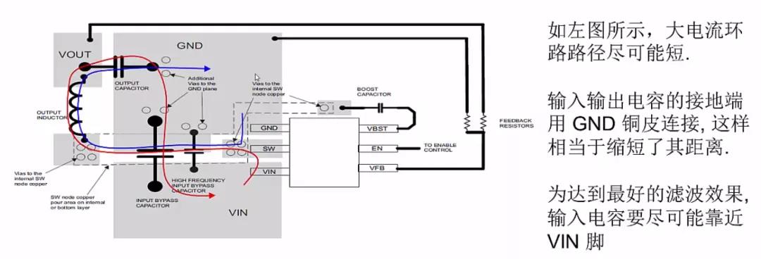
The figure below is the layout of a TI development board. The red is the current path when the upper tube is turned on, and the blue is the current path when the lower tube is turned on. The following layout has the following better advantages:
The GND of the input and output capacitors is connected with copper. When placing the parts, put the grounds of the two together as much as possible;
The current paths at DC-DC Ton and Toff are very short;
The small signal on the right is grounded at a single point, and the distance is relatively long to avoid the influence of the large current switching noise on the left;
The DC-DC PCB layout of a TI development board
3. Examples
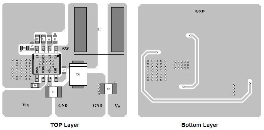
The PCB factory gives the layout of a typical DC-DC BUCK circuit, and the following points are given in SPEC:
The switching loop formed by the input capacitor, high-side MOS tube, and freewheeling diode should be as small and short as possible;
The input capacitor should be as close to Vin Pin as possible;
Ensure that all feedback connections are short and direct, and the feedback resistance and compensation components are as close as possible to the chip;
Keep SW away from sensitive signals, such as FB;
Connect VIN, SW, especially GND to a large copper area to cool the chip and improve thermal performance and long-term reliability;
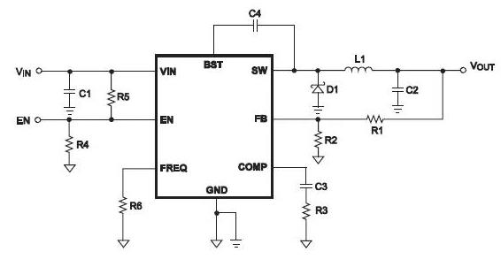
DC-DC BUCK typical circuit layout guide
4. Summary
The layout of the DC-DC circuit is very important and directly affects the stability and performance of the DC-DC. Generally, the SPEC of the DC-DC chip will give layout guidance, which can be referred to for PCB design.