It refers to the microvia (Microvia) with the hole diameter below 6mil and the hole ring diameter (HolePad) below 0.25mm. The contact density is above 130 points/square inch, and the wiring density is above 117 inches/square inch. The printed circuit board hdi circuit board with a width/spacing of 3mil/3mil or less.
Generally speaking, HDI circuit boards have the following advantages:
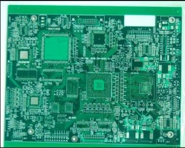
Definition of HDI circuit board
It can reduce the cost of PCB: When the density of PCB increases beyond eight-layer board, it is manufactured with HDI PCB, and its cost will be lower than that of traditional and complex pressing process.
2. Increase circuit density: The interconnection of traditional circuit boards and parts must be connected through the lines and through-hole conductors drawn around the QFP as the connection method (fan-in and fan-out), so these lines need to occupy some space hdi circuit board . The microvia technology can hide the wiring required for interconnection to the next layer. The bonding pads and leads between different layers are directly connected by blind holes in the pads, without fan-in and fan-out wiring. Therefore, some soldering pads (such as mini-BGA or CSP small ball soldering) can be placed on the outer board surface to accept more parts, which can increase the density of the circuit board. At present, many mobile phone boards of high-function small wireless phones use this new type of stacking and wiring method.
3. Conducive to the use of advanced assembly technology: The general traditional drilling technology cannot meet the needs of small parts of the new generation of fine circuit hdi circuit boards due to the size of the pad (through hole) and mechanical drilling. With the advancement of microvia technology, designers can design the latest high-density IC packaging technologies, such as Arraypackage, CSP, and DCA (DirectChipAttach), into the system.

4. Have better electrical performance and signal accuracy: The use of microvia interconnection can not only reduce signal reflection and crosstalk interference between lines, and enable the PCB circuit board circuit design to increase more space, due to the microvia The nature of the physical structure is that the holes are small and short, so the effects of inductance and capacitance can be reduced, and the switching noise during signal transmission can also be reduced.
5. Better reliability: because of the thinner thickness and 1:1 aspect ratio of the micro-hole, the reliability of signal transmission is higher than that of ordinary through-hole hdi circuit boards.
6. Improved thermal properties: The insulating dielectric materials of HDI boards have a higher glass transition temperature (Tg), so HDI circuit boards have better thermal properties.
7. It can improve radio frequency interference/electromagnetic wave interference/electrostatic discharge (RFI/EMI/ESD): the micro-hole technology allows the circuit board designer to shorten the distance between the ground layer and the signal layer to reduce radio frequency interference and electromagnetic wave interference; on the other hand, it can Increase the number of ground wires to avoid instantaneous discharge of parts in the circuit due to static electricity accumulation, and damage to the hdi circuit board.
8. Improve design efficiency: The micro-hole technology allows the circuit to be arranged on the inner layer, so that the circuit designer has more design space, so the efficiency of circuit design can be higher for hdi circuit boards.