HDI board has the following advantages
It can reduce the cost of PCB: When the density of PCB increases to more than eight-layer board, it is manufactured with HDI, and its cost will be lower than that of the traditional and complex pressing process.
Increase circuit density: the interconnection of traditional circuit boards and parts
Conducive to the use of advanced construction technology
Have better electrical performance and signal accuracy
Better reliability
Can improve thermal properties
Can improve radio frequency interference/electromagnetic wave interference/electrostatic discharge (RFI/EMI/ESD)
Increase design efficiency
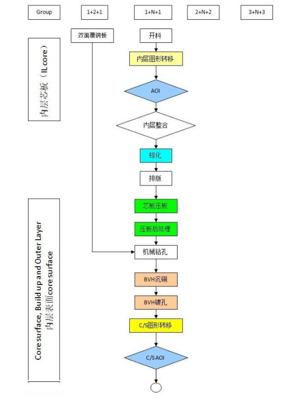
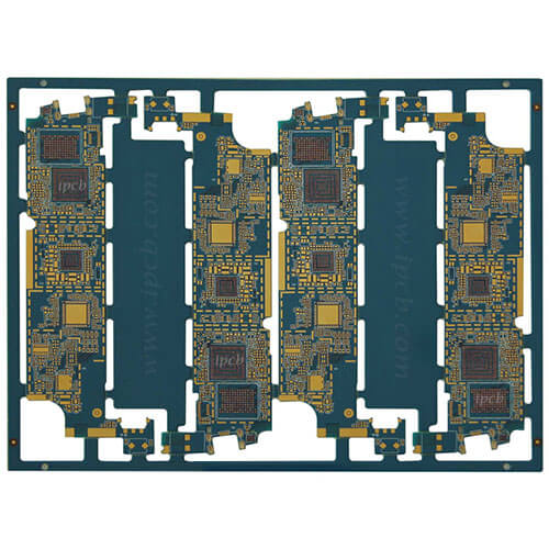
HDI plate imaging
1. While achieving low defect rate and high output, it can achieve the stable production of HDI's conventional high-precision operation. E.g:
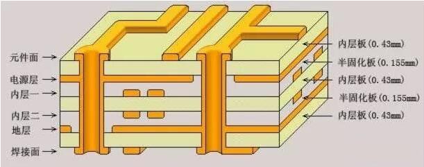
* Advanced board, CSP pitch is less than 0.5mm (connection [with or without wires between discs]
* The board structure is 3+n+3, with three stacked vias on each side,
* 6 to 8 layers coreless PCB printed boards with superimposed vias

In terms of imaging, this type of design requires the ring width to be less than 75mm, and in some cases the ring width is even less than 50mm. Due to alignment issues, these inevitably lead to low production. In addition, driven by miniaturization, lines and pitches are getting finer and thinner-satisfying this challenge requires a change in traditional imaging methods. This can be done by reducing the panel size, or by using a shutter exposure machine for panel imaging in several steps (four or six). Both of these methods achieve better alignment by reducing the influence of material deformation. Changing the panel size has resulted in high material costs, and the use of shutter exposure machines has resulted in low daily output. Neither of these two methods can completely solve the material deformation and reduce the defects related to the photographic plate, which includes the actual deformation of the photographic plate when printing a batch/batch.
2. To achieve the required output by printing the required number of panels every day. As mentioned earlier, the relevant quantity of the required output should be considered in the accuracy requirements. To achieve the required output, automatic control is needed to obtain a high output rate.
3. Low cost operation. This is the main requirement for any mass manufacturer. The early LDI mode either required the traditional use of dry film to be replaced with a more sensitive dry film to achieve faster imaging speed; or according to the light source used in the LDI mode, the dry film was changed to a different waveband. In all these cases, the new dry film is usually more expensive than the traditional dry film used by the manufacturer.
4. Compatible with existing processes and production methods. The processes and methods of mass production are usually carefully regulated to meet mass production requirements. The introduction of any new imaging method should have minimal changes to existing methods. This includes minimal changes in the dry film used, the ability to expose each layer of the solder mask, the traceability function required for mass production, and more.
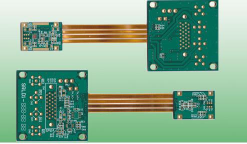
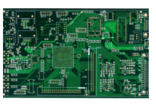
PCB moves toward high-density and refinement, four types of products receive the most attention
At present, PCB products have begun to move from the traditional to higher density HDI/BUM boards,IC packaging base (carrier) boards, embedded component boards and rigid-flex boards. PCB will eventually go to the "printed circuit board". "Limit", in the end, will inevitably lead to a "qualitative change" from "electrical transmission signals" to "optical transmission signals", and printed optical circuit boards will replace printed circuit boards.