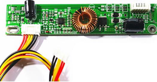
During PCBA processing, there will be many special processes, which will immediately bring restrictions on the PCB boards. If the PCB board does not meet the requirements, it will increase the difficulty of the PCBA soldering process, which may eventually lead to soldering defects and the board is not Qualified, etc. Therefore, in order to ensure the smooth completion of the special process and to facilitate the PCBA processing, the PCB board must meet the manufacturability requirements in terms of size and pad distance. Next, the ipcb processing manufacturer will introduce the PCBA processing to the PCB boards. Requirements.
PCBA processing requirements for PCB boards
1. PCB size
The width of the PCB (including the edge of the board) should be greater than 50mm and less than 460mm, and the length of the PCB (including the edge of the board) should be greater than 50mm. If the size is too small, it needs to be made into a jigsaw.
2. PCB board edge width
Board edge width: >5mm, panel spacing:<8mm, distance="" between="" pad="" and="" board="" edge:="">5mm
3. PCB bending
Upward bending degree:<1.2mm, downward bending degree: <0.5mm, PCB distortion: maximum deformation height ÷ diagonal length <0.25

4.PCB boards mark point
Mark shape: standard circle, square, triangle;
Mark size: 0.8~1.5mm;
Mark material: gold-plated, tin-plated, copper and platinum;
Mark's surface requirements: the surface is flat, smooth, non-oxidized, and free of dirt;
Mark's surrounding requirements: there should be no green oil or other obstacles within 1mm, which is obviously different from the Mark's color;
Mark position: 3mm above the edge of the board, and there should be no Mark-like vias, test points, etc. within 5mm around the board.
5. PCB pads
There are no through holes on the pads of SMD components. If there is a through hole, the solder paste will flow into the hole, resulting in less tin in the device, or the tin flowing to the other side, causing the board surface to be uneven and the solder paste cannot be printed.
When conducting PCB design and production, it is necessary to understand some knowledge of PCBA welding process, so as to make the product suitable for production. Understanding the requirements of the processing plant first can make the subsequent manufacturing process more smooth and avoid unnecessary troubles.
This is the requirement of PCBA processing for PCB boards. When producing PCB boards, do not slacken their efforts. Only by producing high-quality and compliant PCB boards can the boards better accept other special processes, and give the PCB boards life and inject the soul of functionality.
PCBA processing plant
PCBA processing advantages
1. Highly professional: The company focuses on processing samples, small and medium batches, and promises to deliver goods within 3-5 working days after the materials are confirmed.
2. Professional equipment: The company's equipment is advanced equipment tailored for sample and small and medium batch production, which can be attached to 0201, BGA pitch 0.3MM, QFN, CSP, CON and other components.
3. Professional technology: 100% of technical backbones have more than 5 years of work experience, and 85% of frontline operators have more than 3 years of work experience.
4. The company implements the 5S and 6σ concepts in its daily operations, and has at least 7 checks from incoming materials to shipments. Our company promises to pass AOI optical inspection if the quantity reaches 100PCS.
5. The company promises that the welding through rate is over 99%. If the customer finds welding defects, the company promises to repair it free of charge.
PCBA processing
Why choose ipcb?
1. Strength guarantee
▪ SMT workshop: It has imported placement machines and multiple optical inspection equipment, which can produce 4 million points per day. Each process is equipped with QC personnel, who can keep an eye on product quality.
▪ DIP production line: There are two wave soldering machines. Among them, there are more than ten old employees who have worked for more than three years. The workers are highly skilled and can weld all kinds of plug-in materials.
2. Quality assurance, high cost performance
▪ High-end equipment can paste precision shaped parts, BGA, QFN, 0201 materials. It can also be used as a model for mounting and placing bulk materials by hand.
▪ Both samples and large and small batches can be produced. Proofing starts at 800 yuan, and batches start at 0.008 yuan/point, and there is no start-up fee.
3. Rich experience in SMT and soldering of electronic products, stable delivery
▪ Accumulated services to thousands of electronic companies, involving SMT chip processing services for various types of automotive equipment and industrial control motherboards. The products are often exported to Europe and the United States, and the quality can be affirmed by new and old customers.
▪ Delivery on time, normal 3-5 days after the materials are complete, and small batches can also be shipped on the same day.
4. Strong maintenance ability and perfect after-sales service
▪ The maintenance engineer has rich experience and can repair the defective products caused by all kinds of patch welding, and can ensure the connection rate of each PCB boards.
▪ 24-hour customer service staff will respond at any time and solve your order problems as quickly as possible.