ipcb specializes in providing overall PCB electronic manufacturing services, including one-stop services from upstream electronic component procurement to PCB production and processing, SMT patch, DIP plug-in, PCB testing, and finished product assembly. Next, I will introduce the common causes of welding defects in PCB processing.
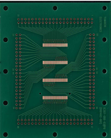
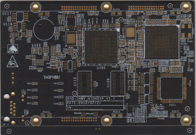
PCB processing manufacturers
Analysis of the Causes of PCB Processing Welding Defects
1. The weldability of the board hole affects the welding quality
The poor solderability of the circuit board holes will result in PCB processing and welding defects, which will affect the parameters of the components in the circuit, resulting in unstable conduction between the multilayer board components and the inner line, resulting in the failure of the entire circuit. The so-called solderability refers to the property that the metal surface is wetted by molten solder, that is, a relatively uniform, continuous and smooth adhesion film is formed on the metal surface of the solder.
The main factors affecting the solderability of printed circuit boards:
(1) The composition of the solder and the properties of the solder. Solder is an important part of the welding chemical treatment process. It is composed of chemicals containing flux. Commonly used low melting point eutectic metals are Sn-Pb or Sn-Pb-ag. The impurity content should be controlled in a certain proportion. In order to prevent the oxides generated by impurities from being dissolved by the flux. The function of the flux is to help the solder to wet the surface of the soldered board by transferring heat and removing rust. White rosin and isopropanol solvents are generally used.

(2) The welding temperature and the cleanliness of the metal plate surface also affect the weldability. When the temperature is too high, the solder spreading speed increases. At this time, the activity is high, the circuit board and the melting surface of the solder are rapidly oxidized, causing solder defects, and the surface of the circuit board is contaminated, which also affects the solderability and causes defects. Including tin beads, tin balls, disconnection, poor gloss, etc.
2. PCB processing welding defects caused by warpage
Circuit boards and components warp during welding, and stress deformation causes PCB processing welding defects such as solder joints and short circuits. Warpage is often caused by the temperature imbalance between the upper and lower parts of the board. For large PCBs, warpage may occur due to the weight of the board itself. Ordinary PBGA devices are about 0.5mm away from the printed circuit board. If the equipment on the circuit board is large, the circuit board will return to its normal shape after cooling, and the solder joints will be stressed for a long time.
3. PCB design affects welding quality
In the PCB design layout, when the size of the circuit board is too large, although the soldering is easier to control, but the printed line is long, the impedance increases, the noise resistance decreases, and the cost increases. String. Mutual interference, such as electromagnetic interference to the board.
Therefore, the PCB design must be optimized:
(1) Shorten the wiring between high-frequency components to reduce electromagnetic interference.
(2) Parts with heavier weight (such as 20g or more) are fixed with brackets and then welded.
(3) Heat dissipation issues should be considered for heating elements to prevent large defects and rework on the surface of the elements. Thermal elements should be kept away from heat sources.
(4) The arrangement of the components is as parallel as possible, which is beautiful and easy to weld, and should be mass-produced. The board is designed as the best 4:3 rectangle. Do not change the line width to avoid intermittent wiring. When the board is heated for a long time, the copper foil is easy to swell and fall off, so avoid large-area copper foil.
SMT factory explains the circuit board processing process in detail
PCB processing capability
1. The largest board: 310mm*410mm (SMT);
2. Maximum board thickness: 3mm;
3. Minimum board thickness: 0.5mm;
4. The smallest Chip parts: 0201 package or parts above 0.6mm*0.3mm;
5. The maximum weight of mounted parts: 150 grams;
6. Maximum part height: 25mm;
7. Maximum part size: 150mm*150mm;
8. Minimum lead part spacing: 0.3mm;
9. The smallest spherical part (BGA) spacing: 0.3mm;
10. The smallest spherical part (BGA) diameter: 0.3mm;
11. Maximum component placement accuracy (100QFP): 25um IPC;
12. Mounting capacity: 3 to 4 million points/day.
PCB processing
Why choose ipcb?
1. Strength guarantee
▪ SMT workshop: It has imported placement machines and multiple optical inspection equipment, which can produce 4 million points per day. Each process is equipped with QC personnel, who can keep an eye on product quality.
▪ DIP production line: There are two wave soldering machines. Among them, there are more than ten old employees who have worked for more than three years. The workers are highly skilled and can weld all kinds of plug-in materials.
2. Quality assurance, high cost performance
▪ High-end equipment can paste precision shaped parts, BGA, QFN, 0201 materials. It can also be used as a model for mounting and placing bulk materials by hand.
3. Rich experience in SMT and soldering of electronic products, stable delivery
▪ Accumulated services to thousands of electronic companies, involving SMT chip processing services for various types of automotive equipment and industrial control motherboards. The products are often exported to Europe and the United States, and the quality can be affirmed by new and old customers.
▪ Delivery on time, normal 3-5 days after the materials are complete, and small batches can also be shipped on the same day.
4. Strong maintenance ability and perfect after-sales service
▪ The maintenance engineer has rich experience and can repair the defective products caused by all kinds of patch welding, and can ensure the connection rate of each circuit board.
▪ 24-hour customer service staff will respond at any time and solve your order problems as quickly as possible.