cause:
The gap between the concave and convex molds is too small, causing cracks to occur on both sides of the convex mold and the concave mold without overlapping, and two extrusion shears occur at both ends of the section.
The gap between the concave and the punch is too large. When the punch is lowered, the cracks will occur late, and the shear will be completed like a tear, causing the cracks to not overlap.
The cutting edge is worn or rounded and chamfered, the cutting edge does not play a role in the division of the wedge, and the entire section has irregular tearing.
Solution
Reasonably choose the blanking gap of the concave and convex dies. Such punching and cutting are between extrusion and stretching. When the punch cuts into the material, the cutting edge forms a wedge, causing the sheet to produce nearly linear coincident cracks.
Refurbish the fillet or chamfer produced by the cutting edge of the concave and convex molds in time.
To ensure the vertical concentricity of the concave and convex molds, so that the matching clearance is even.
To ensure that the mold is installed vertically and smoothly.

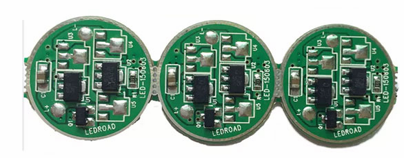
What is the difference between the inner and outer layer etching of PCB circuit board?
The PCB circuit board has many processes and is very particular about its production. The etching methods for the inner and outer layers are different. The obvious difference is that the inner layer generally has a larger line width and line spacing, and the outer layer has a denser line.
Inner layer: developing - etching - peeling
Outer layer: developing-two copper tin plating-stripping-etching-stripping tin
Because the outer line is very dense and the space is not enough, at this time, it is necessary to find a way to achieve the purpose of making the line in the insufficient space. The etching ability can reach 1~2mil ring, but acid etching requires about 5mil, so tin must be used to protect the required circuit first.
It should be noted that PCB circuit boards should not be made where corrosion can be avoided, because the cost of corrosion is higher than that of acid corrosion. The etching factor is the manufacturing capacity of a factory and cannot be improved through the process. The etching ability of acid etching is different.