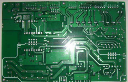
PCB, commonly known as printed circuit board, is an indispensable part of electronic components and plays a core role. In a series of PCB production processes, there are many matching points. If you are not careful, the board will have defects, which will affect your whole body, and PCB quality problems will emerge endlessly. Therefore, after the circuit board manufactured and formed, the inspection test becomes an indispensable link. Let me share with you the faults of PCB circuit boards and their solutions.

1. The PCB board is often delamination in use
Reason: (1) Supplier material or process problem
(2) Poor design material selection and copper surface distribution
(3) The storage time is too long, the storage period is exceeded, and the PCB board is damp
(4) Improper packaging or storage, damp
Countermeasures: Choose the packaging and use constant temperature and humidity equipment for storage. Do a good job of PCB factory reliability test, such as: thermal stress test test in PCB reliability test, the responsible supplier is to use more than 5 times of non-layering as the standard, and it will be confirmed during the sample stage and each cycle of mass production. The general manufacturer may only request 2 times, and only confirm once a few months. The IR test of simulated placement can also prevent the outflow of defective products more, which is a must for an excellent PCB factory. In addition, the Tg of the PCB board should be selected above 145°C, so that it is safer.
Reliability testing equipment: constant temperature and humidity box, stress screening type thermal shock test box, PCB reliability testing equipment
2. The solderability of the PCB board is poor
Reasons: too long storage time, resulting in moisture absorption, contamination and oxidation of the layout, abnormal black nickel, solder resist SCUM (shadow), and solder resist PAD.
Solution: Strictly pay attention to the quality control plan of the PCB factory and the standards for maintenance when purchasing. For example, black nickel, you need to see whether the PCB board production plant has chemical gold, whether the concentration of chemical gold wire is stable, whether the analysis frequency is sufficient, whether there is a regular gold stripping test and phosphorus content test for testing, and whether the internal solderability test is Have good execution and so on.
3. The PCB board is bent and warped
Reasons: unreasonable material selection by the supplier, poor control of heavy industry, improper storage, abnormal operation line, obvious differences in copper area of each layer, and insufficient production of broken holes.
Countermeasures: pressurize the thin board with wood pulp board before packaging and shipping to avoid deformation in the future. If necessary, add a clamp to the patch to prevent the device from bending the board excessively. The PCB needs to simulate the mounting IR conditions for testing before packaging, so as to avoid the undesirable phenomenon of plate bending after the furnace.
4. PCB board impedance is poor
Reason: The impedance difference between PCB batches is relatively large.
Countermeasures: The manufacturer is required to attach batch test reports and impedance strips when delivering, and if necessary, provide comparative data on the inner wire diameter and the side wire diameter of the board.
5. Anti-welding blistering/falling off
Reason: There is a difference in the selection of solder mask inks, the PCB solder mask process is abnormal, caused by heavy industry or excessively high patch temperature.
Countermeasures:PCB suppliers should formulate reliability test requirements for PCB boards and control them in different production processes.
6. The Avani effect
Reason: In the process of OSP and Dajinmian, electrons will dissolve into copper ions, resulting in a difference in potential between gold and copper.
Countermeasures: PCB manufacturers are required to pay close attention to the control of the potential difference between gold and copper in the production process.