There are many types of manufacturing technology for ceramic products in circuit board factories. It is said that there are more than 30 manufacturing process methods, such as dry pressing, grouting, extrusion, injection, casting method and isostatic pressing method, etc., due to electronic ceramics The substrate is a "flat" type (square or wafer method), the shape is not complicated, the manufacturing process of dry molding and processing is simple, and the cost is low, so most of the dry press molding methods are used. The manufacturing process of dry-pressed flat-type electronic ceramics has three main contents, namely blank forming, blank sintering and finishing, and forming a circuit on a substrate.
1. Manufacturing of green parts (forming)
Use high-purity alumina (content ≥95% Al2O3) powder (different particle sizes are required depending on the use and manufacturing method. For example, ranging from a few illiterate to tens of microns) and additives (mainly binders, dispersants, etc.) ) Form a "slurry" or processing material.
(1) The dry pressing method produces green parts (or "green bodies").
The dry pressing blank is to use high-purity alumina (the alumina content for electronic ceramics is greater than 92%, most of which use 99%) powder (the particle size used for dry pressing must not exceed 60μm, and it is used for extrusion The particle size of powders such as, casting, injection, etc. should be controlled within 1 μm) Add appropriate amount of plasticizer and binder, mix well and dry compaction. At present, the offspring of the square or disc can reach 0.50mm, even ≤ 0.3 mm (related to the board size).
The dry-pressed blanks can be processed before sintering, such as the processing of external dimensions and drilling, but attention should be paid to the compensation of the size shrinkage caused by sintering (the size of the enlarged shrinkage rate).
(2) Casting method to manufacture green parts.
Glue fluid (alumina powder + solvent + dispersant + binder + plasticizer, etc. to mix evenly + sieving) manufacturing + casting (apply the glue to metal or heat-resistant polyester on a casting machine) Bringing up) + drying + trimming (holes and other processing can also be carried out) + degreasing + sintering and other processes. Can be automated and large-scale production.
2. Sintering and finishing of green parts. The green parts of ceramic substrates often need to be "sintered" and finished after sintering.
(1) Sintering of green parts.
The “sintering” of the ceramic green body refers to the removal of cavities, air, impurities, and organic matter in the green body (volume) such as dry pressing through the “sintering” process to volatilize, burn, and squeeze, and to remove the alumina particles. The process of achieving close contact or bonding (bonding) to form a long, so after the sintering of the ceramic green body (cooked body), there will be changes in weight loss, size shrinkage, shape deformation, increase in compressive strength, and decrease in porosity. The sintering methods of ceramic green bodies include: 1. normal pressure sintering method, sintering under no pressure will bring about greater deformation, etc.; 2. pressure (hot pressing) sintering method, sintering under pressure, good This is the most commonly used method for flat products; 3. Hot isostatic pressing sintering method uses high-pressure and high-heat gas for sintering. Its characteristic product is a product completed at the same temperature and pressure. Various performances are balanced and the cost is relatively high. This sintering method is often used in value-added products, or aerospace, national defense and military products, such as mirrors, nuclear fuel, gun barrels and other products in the military field.
The sintering temperature of dry pressed alumina green parts is mostly between 1200 degree Celsius and 1600 degree Celsius (related to composition and flux).
(2) Finishing of sintered (cooked) blanks.
Most of the sintered ceramic blanks require finishing. The purpose is: 1. To obtain a flat surface. During the high-temperature sintering process of the green body, due to the imbalance of particle distribution, voids, impurities, organic matter, etc. in the green body, It will cause deformation and unevenness (concave-convex) or excessive roughness and difference, etc. These defects can be solved by surface finishing; 2. Obtain a high smooth surface, like a mirror, or improve lubrication (wear resistance).
The surface polishing treatment is to use polishing materials (such as SiC, B4C) or diamond sand paste to polish the surface step by step from coarse to fine abrasives. Generally speaking, it is mostly achieved by using AlO powder or diamond paste ≤1μm, or processing with laser or ultrasonic.
(3) Strong (steel) treatment.
After the surface is polished, in order to improve the mechanical strength (such as bending strength, etc.), a layer of silicon compound film can be coated by electron beam vacuum coating, sputtering vacuum coating, chemical vapor deposition and other methods, and pass through 1200 degree Celsius ~ Heat treatment at 1600 degree Celsius can significantly improve the mechanical strength of ceramic blanks!

3. The conductive pattern (circuit) is formed on the substrate
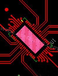
To process and form conductive patterns (circuits) on a ceramic substrate, a copper-clad ceramic substrate must be manufactured first, and then a ceramic printed circuit board is manufactured according to the printed circuit board process technology.
(1) Form a copper-clad ceramic substrate. There are currently two methods for forming copper-clad ceramic substrates.
1. Laminating method. It is formed by hot pressing of copper foil with one side oxidized and alumina ceramic substrate. That is, the ceramic surface is processed (such as laser, plasma, etc.) to obtain an activated or roughened surface, and then laminated together according to "copper foil + heat-resistant adhesive layer + ceramic + heat-resistant adhesive layer + copper foil", After sintering at 1020°C ~ 1060°C, a double-sided copper-clad ceramic laminate is formed.
2. Plating method. After the ceramic substrate is processed by plasma, "sputtered titanium film + sputtered nickel film + sputtered copper film, then conventionally electroplated copper to the required copper thickness, that is, a double-sided copper-clad ceramic substrate is formed.
(2) Manufacturing of single and double-sided ceramic PCB boards. Single and double-sided copper-clad ceramic substrates are used in accordance with conventional PCB manufacturing technology.
(3) Manufacturing of ceramic multilayer boards.
1. Single and double-sided boards are repeatedly coated with insulating layer (alumina), sintered, wired, and sintered to form a multilayer board, or completed by tape casting technology.
2. Ceramic multilayer board is manufactured by casting method. The green tape is formed on the casting machine, and then drilled, plugged (conductive glue, etc.), printed (conductive circuit, etc.), cut, laminated and isostatically pressed to form a ceramic multilayer board. Figure 1 shows the completed multilayer ceramic chip capacitor.
Note: Casting molding method-glue liquid (alumina powder + solvent + dispersant + binder + plasticizer, etc. mixed evenly + sieving) manufacturing + casting (distribute the glue evenly on the casting machine Coated on metal or heat-resistant polyester tape) + drying + trimming + degreasing + sintering and other processes.
In short, ceramic printed boards belong to the category of PCBs, and are also the result of the derivation and extension of the development and progress of PCB factories. In the future, they may form one of the important types in the PCB field. Since ceramic printed boards have the best thermal conductivity insulating medium, high melting point and thermal dimensional stability, ceramic PCBs will have broad development prospects in the application of high temperature and high thermal conductivity!