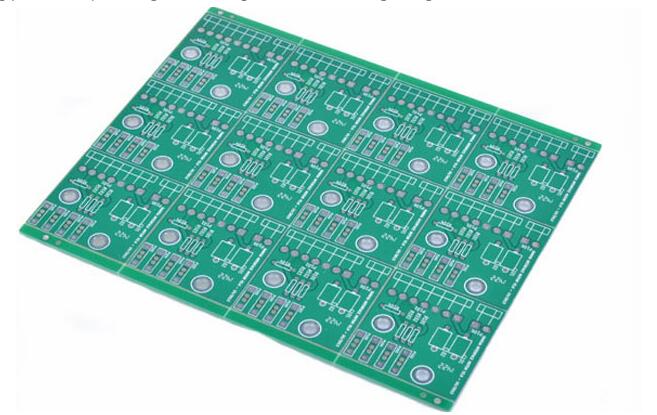
Because some PCB circuit boards are relatively small, they are often designed into an imposition method, which not only facilitates the processing and production of the electronics factory, but also reduces the waste of the board and reduces the cost. In order to facilitate circuit board manufacturing and PCBA processing, many issues need to be paid attention to when PCB imposition design is carried out.

Matters needing attention in PCB imposition design
In order to facilitate production, PCB circuit board imposition generally needs to design Mark points, V-grooves, and process edges.
1. Imposition shape
1. The outer frame (clamping edge) of the PCB jigsaw should adopt a closed loop design to ensure that the PCB jigsaw will not be deformed after being fixed on the fixture.
2. PCB board width ≤260mm (SIEMENS line) or ≤300mm (FUJI line); if automatic dispensing is required, PCB board width*length ≤125 mm*180 mm.
3. The shape of the PCB jigsaw should be as close to the square as possible, and 2*2, 3*3, …… jigsaw is recommended; but do not put together a yin and yang board;
2. V-groove
1. After opening the V-groove, the remaining thickness X should be (1/4~1/3) the plate thickness L, but the minimum thickness X must be ≥0.4mm. The upper limit can be taken for heavy-bearing boards, and the lower limit can be taken off for light-bearing boards.
2. The misalignment S of the cuts on the upper and lower sides of the V-groove should be less than 0.1mm; due to the limitation of the minimum effective thickness, it is not suitable to use the V-groove splicing method for the board with the thickness less than 1.2mm.
3. Mark point
1. When setting the reference positioning point, usually leave a non-resistance area 1.5 mm larger than it around the positioning point.
2. It is used to help the optical positioning of the placement machine. There are at least two asymmetric reference points on the diagonal of the PCB board with patch devices. The reference points for the optical positioning of the entire PCB are generally at the corresponding diagonal positions of the entire PCB; divided PCB The reference point for optical positioning is generally at the corresponding position on the diagonal of the divided PCB circuit board.
3. For QFP (quad flat package) with lead pitch ≤0.5mm and BGA (ball grid array package) with ball pitch ≤0.8mm, in order to improve placement accuracy, it is required to set reference points on the two opposite corners of the IC.
Fourth, the craft side
1. There should be no large devices or protruding devices near the connection point between the frame of the jigsaw frame and the internal small board, between the small board and the small board, and there should be more than 0.5mm space between the components and the edge of the PCB circuit board., To ensure the normal operation of the cutting tool.
5. Positioning holes on the board
1. The reference symbol used for the positioning of the entire PCB circuit board and the positioning of fine-pitch devices. In principle, the QFP with a spacing of less than 0.65mm should be set at its diagonal position; the positioning reference symbol used for the imposition PCB sub-board should be Used in pairs, arranged at the opposite corners of the positioning elements.
2. Large components should have positioning posts or positioning holes, such as I/O ports, microphones, battery ports, micro switches, earphone ports, motors, etc.
A good PCB designer should consider production factors when making imposition design, so as to facilitate processing, improve production efficiency, and reduce production costs.