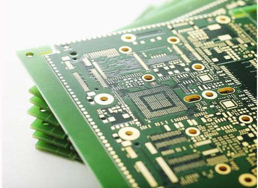
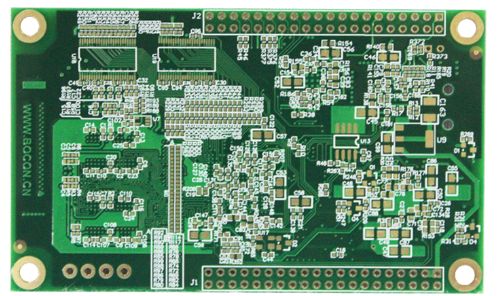
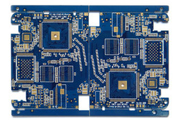
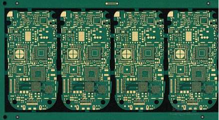
Six-layer PCB conventional laminated structure introduction
The laminated structure of PCB is an important factor that affects its EMC performance, and it is also an important means to suppress electromagnetic interference. Before multi-layer PCB board design, it is necessary to determine the circuit board structure used according to the circuit scale, circuit board size and electromagnetic compatibility (EMC) requirements. The editor of the PCB factory will use this article to introduce the knowledge about the conventional laminated structure of the six-layer PCB.
In some six-layer PCB design stacking schemes, the shielding effect of electromagnetic fields is not good enough, and the effect of reducing the transient signal of the power bus is also minimal. For the design with higher chip density and higher clock frequency, a six-layer PCB design can be considered.

The first laminated scheme: SIG-GND-SIG-PWR-GND-SIG;
This layered solution can get better signal integrity, the signal layer is adjacent to the ground layer, the power layer and the ground layer are paired, the impedance of each wiring layer can be better controlled, and both ground layers can be good Absorb the lines of magnetic force. In addition, it can provide a better return path for each signal layer when the power and ground layers are complete.
The second stacking scheme: GND-SIG-GND-PWR-SIG -GND;
This laminate solution is only suitable for the case where the device density is not very high. This laminate has all the advantages of the upper laminate, and the ground planes of the top and bottom layers are relatively complete and can be used as a better shielding layer. . It should be noted that the power layer should be close to the layer that is not the main component surface, because the plane of the bottom layer will be more complete. Therefore, the EMI performance is better than the first solution.
For the six-layer PCB design, in order to obtain better power and ground coupling, the distance between the power layer and the ground layer should be minimized. Like the 62mil board thickness, although the layer spacing is reduced, it is not easy to control the spacing between the main power supply and the ground layer to be small. Compared with the first solution, the second solution greatly increases the cost, so we generally choose the first solution when stacking. When designing, follow the 20H rule and the mirror layer rule design.
The above is the introduction to the related knowledge of the six-layer PCB conventional laminated structure, I hope it will be helpful to you!