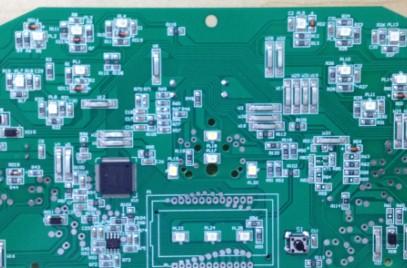
Light painting refers to the laser light plotter exposing the required part of the film on the film, and the pattern will appear after washing. The same is true for using such a film to make the pattern on the PCB board. The pattern is transferred by exposure.
Ordinary double-panel process: cutting material "drilling" copper thickening "outer layer graphics" external image inspection "solder mask" solder mask inspection "character" surface treatment "molding" testing "drawing test lines" FQC "FQA" packaging Shipment

PCBlight painting to check user's files
1. Check whether the file is in good condition;
2. Check whether the file is poisonous, if it is poisonous, it must be disinfected first;
3. If it is a Gerber file, check whether there is a D code table or contains D code.
Check whether it meets the technical level of our factory
1. Check whether the various spacings of the PCB design in the customer files are in line with the factory process: the spacing between the lines, the spacing between the lines and the pads, the spacing between the pads and the pads. The above various spacings should be greater than the minimum spacing that can be achieved by the factory's production process.
2. Check the width of the wire. The width of the wire should be greater than the minimum line width that can be achieved by the factory's production process.
3. Check the size of the via hole to ensure the smallest diameter of the factory's production process.
4. Check the size of the pad and its internal aperture to ensure that the edge of the pad after drilling has a certain width.
PCB light painting to determine process requirements
Process requirements:
1. Different requirements of the subsequent process, determine whether the PCB light painting film (commonly known as film) is mirrored. The principle of negative film mirroring: the medicated film surface (ie, the glue surface) is attached to the medicated film surface to reduce the error. The determinant of the mirror image: craftsmanship. If it is a screen printing process or a dry film process, the copper surface of the substrate on the film side of the film shall prevail. If the diazo film is used for exposure, since the diazo film is a mirror image when copied, its mirror image should be the film surface of the negative film without the copper surface of the substrate. If the PCB light-painting is a unit film instead of imposition on the PCB light-painting film, one more mirroring is required.
2. Determine the parameters for solder mask expansion.
Determine the principle:
1. Do not expose the wire next to the pad.
2. Small can't cover the pad.
Due to errors during operation, the solder mask may have deviations on the circuit. If the solder mask is too small, the result of the deviation may mask the edge of the pad. Therefore, the solder mask should be larger. But if the solder mask is enlarged too much, the wires next to it may be exposed due to the influence of deviation.
Convert CAD files to Gerber files during PCB light painting
In order to perform unified management in the CAM process, all CAD files should be converted to the standard format Gerber of the PCB light plotter and the equivalent D code table.
During the conversion, attention should be paid to the required process parameters, because some requirements are to be completed during the conversion.
All kinds of CAD software in common use, except PCB Work and Tango software, can be converted to Gerber. The above two softwares can also be converted to Protel format through tool software, and then to Gerber.