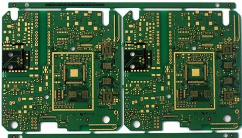
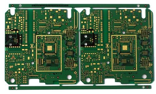
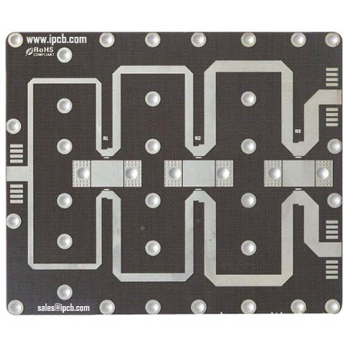
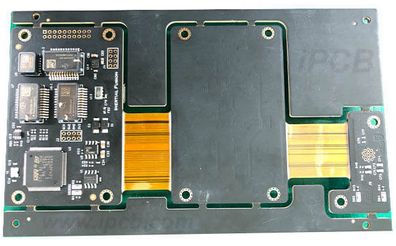
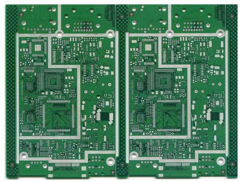
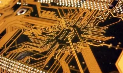
PCB is an important electronic component, and it is the origin of all electronic components. It has become more and more complicated since it first appeared in the last world. From single layer to double layer, four layer, and then to multiple layers, the design difficulty has become more and more difficult. Bigger. There are wiring on both sides of the double panel, which is very helpful for us to understand and master its wiring principle. Let's take a look at the wiring principle of the PCB double board.
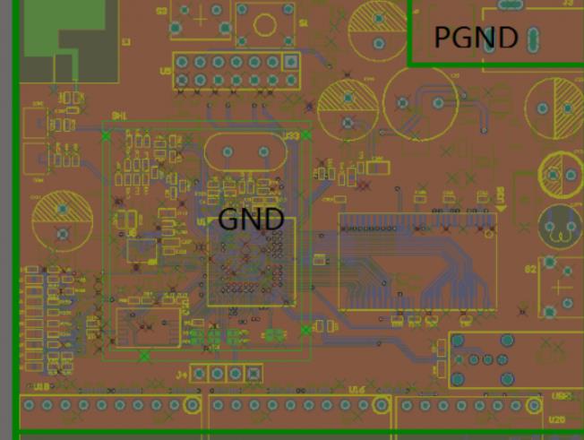
The PCB grounding double board is designed to surround the box-shaped fence, that is, the PCB side is laid more parallel to the ground, and the other side is the vertical grounding wire copy board, and then they are cross-connected with the metalized vias (the through-hole resistance is small).
Taking into account that there should be a grounding wire near each IC chip, usually one grounding wire is made every 1~115cm, which will make the area of the signal loop smaller and help reduce radiation. The network design method should be before the signal line, otherwise it will be difficult Implement.

Principle of signal wire wiring:
After determining the reasonable layout of the components, then the double-layer board, then the design of the ground shielding wire, and then the important wires (sensitive wires, high-frequency wires and rear-laying ordinary wires). The key wire must have a separate power supply, ground wire loop, and the wire is very short, so sometimes the ground wire near the key wire is close to the signal wire, so that the smallest working loop can be formed.
The four-layer board has a double top surface, and the bottom of the wiring board is the signal line. First of all, the key crystal cloth, crystal circuit, clock circuit, signal line and other CPU must comply with the principle of the smallest possible circulation area.
When the printing plate IC circuit is working, the circulation area is mentioned many times, which is actually the concept of differential mode radiation. For example, the definition of differential mode radiation: the working current of the circuit flows in the signal circuit, and the signal loop will generate electromagnetic radiation, which is caused by the current differential mode. Therefore, the differential mode signal loop is called radiated radiation, and the intensity of the radiated field The calculation formula is: E1 = K1, f2, ia / gamma

Type: E1-Differential mode copy board, the spatial gamma radiation field intensity of PCB circuit can be seen by the differential mode radiation formula, the radiation field intensity is proportional to the working frequency f2, the flow area of A, and the working current. I like to determine when to work The frequency f and the size of the flow area are the key factors that we can directly control the design. At the same time, the flow work only needs to meet the reliability, speed, and current. Wider, the higher the electromagnetic radiation, you must point out (above) the greater the power of its current, which is what we do not want.
If possible, use ground wires around key connections. When wiring the PCB copy board in succession, the available ground wires cover all the gaps, but all these ground wires must be paid attention to. The grounding will form a short and large low impedance coupling, so that good results can be obtained (note: there is a space requirement that must be met Conditions, such as creepage distance).