[Inner circuit] The copper foil substrate is first cut into a size suitable for processing and production. Before laminating the substrate, it is usually necessary to properly roughen the copper foil on the surface of the board by brushing, microetching, etc., and then attach the dry film photoresist tightly to it at an appropriate temperature and pressure. Send the dry film photoresist substrate to the UV exposure machine for exposure. The photoresist will polymerize after being irradiated by ultraviolet rays in the light-transmitting area of the film, and the circuit image on the film will be transferred to the dry film photoresist on the board. . After tearing off the protective film on the film surface, first use sodium carbonate aqueous solution to develop and remove the unlit area on the film surface, and then use the hydrogen peroxide mixed solution to corrode and remove the exposed copper foil to form a circuit. Finally, the dry film photoresist that has worked well is washed away with a lightly oxidized sodium water solution.
Special half hole craft.jpg
[Pressing] The inner circuit board after completion must be bonded with the outer circuit copper foil with glass fiber resin film. Before pressing, the inner layer board needs to be blackened (oxidized) to passivate the copper surface to increase the insulation; and the copper surface of the inner layer circuit is roughened in order to produce good adhesion to the film. When stacking, first riveting the inner circuit boards of six layers (including) with a riveting machine in pairs. Then use a tray to neatly stack it between the mirror steel plates, and send it to a vacuum laminator to harden and bond the film with proper temperature and pressure. After pressing the circuit board, the target hole is drilled by the X-ray automatic positioning target drilling machine as the reference hole for the alignment of the inner and outer layers. And make appropriate fine cutting of the edge of the board to facilitate subsequent processing.
[Drilling] The circuit board is drilled with a CNC drilling machine to drill the through holes of the interlayer circuit and the fixing holes of the welding parts. When drilling, use the pin to fix the circuit board on the drilling machine table through the previously drilled target hole, and add a flat bottom plate (phenolic resin board or wood pulp board) and upper cover plate (aluminum plate) at the same time In order to reduce the occurrence of drilling hair.

[Plated through holes] After the interlayer vias are formed, a metal copper layer needs to be laid on them to complete the interlayer circuit conduction. First, use heavy brushing and high-pressure washing to clean the hair on the hole and the dust in the hole, and soak and adhere tin on the cleaned hole wall.
[One-time copper] Palladium colloidal layer, and then reduce it to metallic palladium. The circuit board is immersed in a chemical copper solution, and the copper ions in the solution are reduced and deposited on the wall of the hole by the catalytic action of palladium metal to form a through-hole circuit. Then, the copper layer in the via hole is thickened by copper sulfate bath electroplating to a thickness sufficient to resist the impact of subsequent processing and use environment.
[Outer circuit secondary copper] The production of the circuit image transfer is the same as the inner circuit, but the circuit etching is divided into two production methods, positive film and negative film. The production method of the negative film is the same as the production of the inner layer circuit. After the development, the copper is directly etched and the film is removed. The production method of the positive film is to add copper and tin-lead twice after development (the tin-lead in this area will be retained as an etching resist in the later copper etching step), and after removing the film, use alkaline The mixed solution of ammonia water and copper chloride corrodes and removes the exposed copper foil to form a circuit. Finally, the tin-lead stripping solution is used to strip the tin-lead layer that has worked out (in the early days, the tin-lead layer was retained and used to coat the circuit as a protective layer after re-wrapping, but it is mostly not used now).
[Solder Resistant Ink, Text Printing] The earlier green paint was produced by direct thermal drying (or ultraviolet irradiation) after screen printing to harden the paint film. However, because it often causes green paint to penetrate the copper surface of the circuit terminal contact during the printing and hardening process, which causes problems in welding and use of parts, now in addition to the use of simple and rough circuit boards, photosensitive green paint is often used. in production.
Print the text, trademark or part number required by the customer on the surface of the board by screen printing, and then heat the text (or ultraviolet radiation) to harden the text lacquer ink.
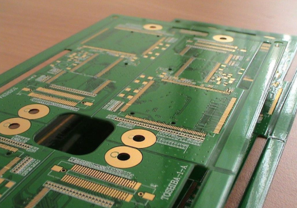
[Contact processing] The solder mask green paint covers most of the copper surface of the circuit, and only the terminal contacts for part welding, electrical testing and circuit board insertion are exposed. This terminal needs to be added with a proper protective layer to avoid oxides generated at the terminal connected to the anode (+) during long-term use, which will affect the stability of the circuit and cause safety concerns.
[Forming and cutting] The circuit board is cut into the external size required by the customer with a CNC molding machine (or die punch). When cutting, a pin is used to fix the circuit board on the bed (or mold) to form through the previously drilled positioning hole. After cutting, the golden finger parts are then processed to beveled to facilitate the use of the circuit board. For multi-piece molded circuit boards, X-shaped break lines are often required to facilitate customers' splitting and dismantling after plug-in. Finally, clean the dust on the circuit board and the ionic contaminants on the surface.