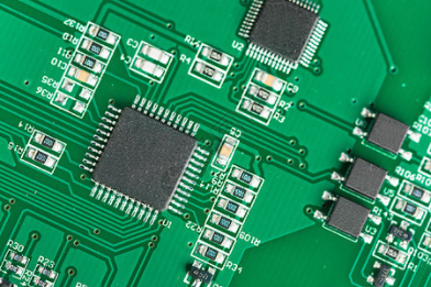
The circuit board factory explains the impedance control of the PCB circuit board for you in detail
Circuit board factory: 1. What is characteristic impedance?
The resistance of high-frequency signals or electromagnetic waves during transmission of electronic equipment signal transmission lines is the characteristic impedance. Its symbol is Zo, referred to as impedance.
Impedance control 2. Definition of impedance control
It means that the customer has requirements for the control of the characteristic impedance of the board, and after calculating according to the impedance calculation formula, measures must be taken to control the impedance on the PCB board so that it is within a certain range (tolerance).
Impedance test range: 50-150Ω; single line: 50Ω/75Ω; paired line: 90Ω/100Ω/125Ω.
The current impedance control tolerance is within 10% or even 5%, which is quite difficult.
Third, the definition of signal transmission line

When the signal is transmitted in the PCB wire, if the length of the wire is not less than 1/7 of the signal wavelength, the wire at this time becomes a signal transmission line. For signal transmission lines, if the characteristic impedance of the line is improperly controlled, the signal will be reflected (or partially reflected) back, making the signal unable to be transmitted or interfered. Therefore, in order to maintain the integrity, reliability, accuracy, interference and noise of the transmission signal, high-precision control of the characteristic impedance is required.
Four, impedance type
There are four types of impedance, and the order of difficulty is from difficult to easy to control: inner double wire> outer double wire> outer cover solder resist single wire impedance> inner single wire impedance.
When calculating the inner two-wire impedance transmission line that is the most difficult to process, there are usually two ways:
1. Microstrip line: It is widely used in practice. Its outer layer is a signal line surface that controls impedance, and it is separated from the adjacent reference surface with an insulating material.
2. Strip line: refers to the thin wire embedded between two AC ground layers. Compared with the microstrip line, the electronic coupling between each layer of the circuit and the ground layer is closer, and the crosstalk between the currents will be lower.
Five, the main factors affecting characteristic impedance
The main factors include dielectric constant, dielectric thickness, wire width, wire thickness, solder mask thickness, etc. Studies have shown that the characteristic impedance is also affected by the thickness of the solder resist ink. Therefore, it is necessary to select the substrate material of the PCB board, the copper clad plate (the thickness of the copper foil), the material of the dielectric layer prepreg (dielectric constant), and the ink before designing.
1. Dielectric constant
The dielectric constant is determined by the measurement of the material at a certain frequency (such as 1MHz); the same material produced by different manufacturers has different dielectric constants due to different resin content.
2. Media thickness
The characteristic impedance is proportional to the natural logarithm of the dielectric thickness, and the characteristic impedance value increases with the increase of the dielectric thickness. Even under the same dielectric thickness and material, the design of the microstrip line structure has a higher characteristic impedance than the strip line design The value is generally larger than 20-40Ω. Therefore, for high-frequency and high-speed digital signal transmission, microstrip line structure design is mostly adopted.
3. Wire thickness
The thickness of the wire is equal to the thickness of the base copper plus the thickness of the plating layer. The greater the thickness of the wire, the smaller its characteristic impedance, but the effect is relatively small.
The thickness of the wire is mainly affected by the following factors:
(1) The thickness of the base copper foil.
(2) The mechanical brushing and micro-etching in the pretreatment will make the copper thickness thinner.
(3) Electroplating will thicken copper.
4. Line width
After the PCB design is completed, the three parameters of dielectric constant, dielectric width and wire thickness are basically relatively fixed; and the wire width is completely processed in the PCB production process. Changing and controlling the line width is the most fundamental way and method to control the PCB characteristic impedance value and variation range.
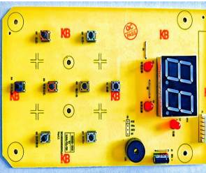
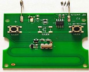
ipcb is a high-precision, high-quality PCB manufacturer, such as: isola 370hr PCB, high-frequency PCB, high-speed PCB, ic substrate, ic test board, impedance PCB, HDI PCB, Rigid-Flex PCB, buried blind PCB, advanced PCB, microwave PCB, telfon PCB and other ipcb are good at PCB manufacturing.