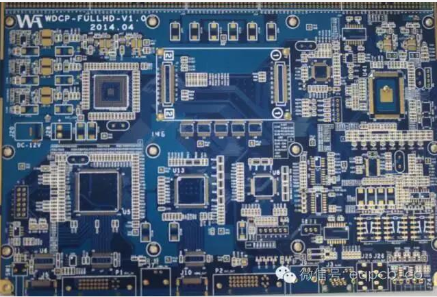
The PCB high-frequency board is made of different components and a variety of complex process technologies. Among them, the structure of the PCB high-frequency board has a single-layer, double-layer, and multi-layer structure. Different layer structures have different production methods.
This article will introduce in detail: the names and corresponding uses of the components of the PCB circuit board, the production of single-layer, double-layer, and multi-layer structures of the PCB high-frequency board, and the main functions of various types of work levels.
First, the common PCB high-frequency board layer structures of printed circuit boards include single-layer boards (SingleLayerPCB), double-layer boards (DoubleLayerPCB) and multi-layer boards (MultiLayerPCB). A brief description of these three board layer structures is as follows:
1. Single-sided board of high-frequency board: that is, a high-frequency board/circuit board with copper on one side and no copper on the other side. Usually components are placed on the side without copper, and the side with copper is mainly used for wiring and soldering.
2. High-frequency board double-layer board: a circuit board with copper on both sides, usually called the top layer (TopLayer) on one side, and the bottom layer (BottomLayer) on the other side. Generally, the top layer is used as the surface for placing components, and the bottom layer is used as the welding surface for components.
3. High-frequency board multi-layer circuit board: a high-frequency board/circuit board that contains multiple working layers. In addition to the top and bottom layers, it also contains several intermediate layers. Usually the intermediate layers can be used as wire layers, signal layers, power layers, and grounding layers. Layers and so on. The layers are insulated from each other, and the connection between the layers is usually achieved through vias.

2, the printed circuit board/high frequency board is mainly composed of pads, vias, mounting holes, wires, components, connectors, filling, electrical boundaries, etc. The main functions of each component are as follows:
Pad: A metal hole used to solder the pins of components.
Via: A metal hole used to connect the pins of components between layers.
Mounting hole: used to fix the printed circuit board.
Wire: The copper film of the electrical network used to connect the pins of the components.
Connectors: components used for connection between high-frequency boards/circuit boards.
Filling: Copper coating for ground wire network, which can effectively reduce impedance.
Electrical boundary: used to determine the size of the high-frequency board/circuit board, and all components on the high-frequency board/circuit board cannot exceed the boundary.
Third, the printed circuit board includes many types of working layers, such as signal layer, protective layer, silk screen layer, internal layer, etc. The functions of each layer are briefly introduced as follows:
1. Signal layer: Mainly used to place components or wiring. ProtelDXP usually contains 30 middle layers, namely MidLayer1~MidLayer30. The middle layer is used to arrange signal lines, and the top and bottom layers are used to place components or deposit copper.
2. Protection layer: It is mainly used to ensure that the high-frequency board does not need to be tinned, so as to ensure the reliability of the circuit board operation. Among them, TopPaste and BottomPaste are the top solder mask and the bottom solder mask respectively; TopSolder and BottomSolder are the solder paste protection layer and the bottom solder paste protection layer, respectively.
3. Silk screen layer: mainly used to print the serial number, production number, company name, etc. of the components on the printed circuit board.
4. Internal layer: Mainly used as signal wiring layer. Protel 99SE and DXP include 16 internal layers.
5. Other layers: mainly include 4 types of layers.
DrillGuide (drilling azimuth layer): Mainly used for the position of drilling holes on printed circuit boards/high-frequency boards.
The above is the introduction of the composition and some of the main functions of the PCB high-frequency board that the ipcb editor and you have learned together, I hope to help you.