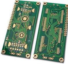
Except for the pin holes, mechanical holes, heat dissipation holes and test holes of the various through holes of PCB high-frequency circuit boards, other via holes (such as ViaHole) need not be exposed, all require solder mask plug holes, especially HDI high density. The connection technology is becoming more and more dense. There are more and more VIP holes and VBP holes on PCB high-frequency circuit boards for packaging, and more and more via plugs are required. So what are the advantages of using solder masks? Next, the editor of Shenzhen Mingchengxin Circuit will introduce the seven advantages of PCB high-frequency circuit board solder mask green oil plug holes.
The green oil plug hole is to plug the green oil into the via hole, which is generally filled with two-thirds of it, and it is better not to transmit light. Generally, if the via hole is large, the size of the ink plug hole is different according to the manufacturing capacity of the PCB high-frequency circuit board factory. Generally, the hole below 16mil can be plugged, and the larger hole should be considered by the PCB high-frequency circuit board factory. Can it be plugged?

1. PCB high-frequency circuit board plug holes can prevent possible short circuits caused by fine-pitch devices (such as BGA). This is the reason for the via fortress hole under the BGA in the design process. Because there is no plug hole, there is a case of short circuit.
2. Avoid flux residue in the vias.
3. The plug hole will help the SMT process to a certain extent.
4. Prevent the tin bead from popping up during wave soldering, causing short circuit.
5. Prevent the surface solder paste from flowing into the hole and cause false soldering, which affects the placement; this is most obvious in the heat dissipation pad and the via hole.
6. After the surface mounting of the electronics factory and the assembly of the components are completed, the PCB high-frequency circuit board must be vacuumed to form a negative pressure on the testing machine to complete.
7. The plug hole can prevent the PCB high-frequency circuit board from being short-circuited by the through hole through the component surface when the PCB high-frequency circuit board passes through the component surface; this means that there is no via hole in the range of the wave soldering design area (generally the soldering surface is 5mm or more) Or it is the reason why the via is plugged