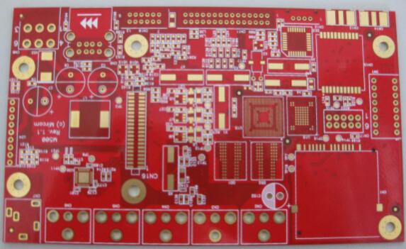
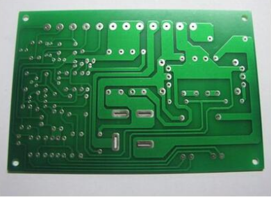
What are the processes of the ceramic substrate etching process?
In PCB proofing, etching is a very important process in the ceramic substrate PCB proofing process. Let me share with you the ceramic substrate etching process:
The etching of the ceramic substrate refers to pre-plating a layer of lead-tin anti-corrosion layer on the circuit pattern, and then chemically etching away the unprotected non-conductor part of the copper to form a circuit. Etching is divided into inner layer etching and outer layer etching. The inner layer etching adopts acid etching, using wet film or dry film as the resist, which has the advantages of easy control of the etching speed, high copper etching efficiency, good quality, and easy recycling of the etching solution. And other characteristics; the outer layer etching adopts alkaline etching, and tin-lead is used as a resist.
1. The alkaline etching process of ceramic substrate is as follows:
1. Film fading: Use the film fading solution to remove the film on the circuit board surface, exposing the unprocessed copper surface.
2. Etching: Use the etching solution to etch away the unnecessary bottom copper, leaving a thicker circuit. Among them, additives, revetment agents, and depressants are used.
Note: The accelerator is used to promote the oxidation reaction and prevent the precipitation of cuprous ions; the bank protection agent is used to reduce the side corrosion; the suppressor is used to suppress the dispersion of ammonia, the precipitation of copper and accelerate the oxidation reaction of the corroded copper.
3. New lotion: Use ammonium monohydrate without copper ions, and use ammonium chloride solution to remove the remaining liquid on the board.
4. Hole: This process is only suitable for immersion gold process. It mainly removes excess palladium ions in non-plated through holes to prevent gold ions from being deposited in the gold immersion process.
5. Dissolving tin: Use nitric acid solution to dissolve the tin-lead layer.

2. Acidic copper chloride etching process for ceramic-based circuit boards
1. Development: Use sodium carbonate to dissolve the part of the dry film that has not been irradiated with ultraviolet rays, and the part that has been irradiated is retained.
2. Etching: According to a certain proportion of the solution, dissolve the exposed copper surface after dissolving the dry film or the wet film with an acidic copper chloride etching solution.
3. Film fading: Dissolve the protective film on the line according to a certain proportion of the potion under a specific temperature and speed environment.
The above is the description of the etching process in the ceramic substrate PCB proofing shared by the editor of the PCB factory. In PCB proofing, the PCB proofing of ceramic substrates is a special process, which has high technical requirements.