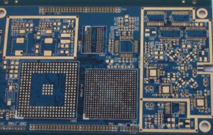
This article focuses on the concepts and planning principles of microwave-level high-frequency circuits/microwave circuits and their high-frequency PCB board planning in a frontier area of communication products. The reason why the microwave-level high-frequency circuit/microwave circuit's high-frequency PCB board planning principle was selected is because this principle has extensive guiding significance and is a popular high-tech application technology at that time. The transition from the planning concept of the microwave circuit high-frequency PCB board to the high-speed wireless network (including various access networks) projects is also connected in the same vein, because they are based on the same fundamental principle and the double transmission line theory.
Experienced high-frequency microwave RF engineers plan digital circuits or relatively low-frequency circuits high-frequency PCB boards, the first-time success rate is very high, because their planning concept is centered on "distributed" parameters, and the concept of distributed parameters is The destructive effects in lower frequency circuits (including digital circuits) are often overlooked.
For a long time, many electronic products (mainly for communication products) that many peers have finished planning have often been problematic. On the one hand, of course, it is related to the lack of necessary links in electrical principle planning (including redundancy planning, reliability planning, etc.), but more importantly, many such problems are caused when people think that all necessary links have been considered. . In response to these problems, they often spend their energy on checking procedures, electrical principles, parameter redundancy, etc., but seldom spend their energy on reviewing high-frequency PCB board planning, and it is often because of high-frequency PCB. Board planning defects have caused a lot of product function problems.

The planning principles of high-frequency PCB boards involve many aspects, including various fundamental principles, anti-interference, electromagnetic compatibility, safety protection, and so on. Regarding these aspects, especially in high-frequency circuits/microwave circuits (especially in microwave-level high-frequency circuits), the lack of related concepts often leads to the failure of the entire R&D project. Many people still stay on the basis of "connecting electrical principles with conductors to play a predetermined effect", and even think that "high-frequency PCB board planning is attributed to the considerations of structure, process, and improvement of production power." Many professional high-frequency microwave radio frequency engineers have not fully realized that this link in the radio frequency planning should be the special key to the entire high-frequency PCB board planning operation, and mistakenly spent energy on selecting high-function components. The result is a huge cost. Ascends, the functional progress is minimal.
It should be particularly pointed out here that the digital circuit relies on its strong anti-interference, error detection and correction, and arbitrary structure of various intelligent links to ensure the normal function of the circuit. A general digital application circuit and the high additional configuration of various "guarantee normal" links are obviously attributed to actions without product concepts. But often in the link that is considered "not worthwhile", it leads to product series problems. The reason is that this kind of functional links that are not worthy of structural reliability assurance from the product engineering point of view should be based on the operating mechanism of the digital circuit itself. It is only the error structure in the circuit planning (including the high-frequency PCB board planning) that causes the circuit to be in An unstable situation. This instability causes similar problems with high-frequency circuits/microwave circuits to be attributed to the fundamental application of the same concept.
In digital circuits, there are three aspects worth taking seriously:
1. Various reliability plans in the application of digital circuits are related to the reliability requirements of the circuit in actual use and product engineering requirements. It is not possible to attach various high-cost "guarantees" to circuits that can fully meet the requirements using conventional planning.
2. The operating speed of digital circuits is moving towards high frequency with unprecedented development (for example, the current CPU, whose main frequency has reached 1.7GHz, has far exceeded the lower limit of the microwave frequency band). Although the reliability assurance functions of related devices are also matched, they are based on the internal and typical external signal characteristics of the device.
3. The digital signal itself is classified as a broad-spectrum signal. According to the results of the Fourier function, the high-frequency components contained in it are very rich, so the high-frequency weight of the digital signal is fully considered in the planning of the digital IC. However, in addition to digital IC, the signal transition area within and between each function link, if it is arbitrarily done, will cause a series of problems. Especially in circuits where digital and analog and high-frequency circuits (high-frequency PCB boards) are mixed.