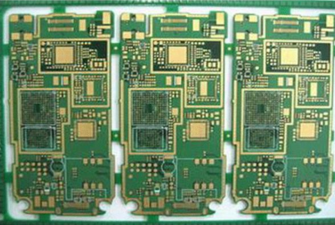
(1) The package of the components used on the PCB must be correct, including the size and size of the component pins, the spacing of the pins, the number of the pins, the size and direction of the frame, etc.
(2) The positive and negative poles or pin numbers of polar components (electrolytic capacitors, diodes, triodes, etc.) should be marked in the PCB component library and on the PCB board.
(3) The pin numbers of the components in the PCB library should be consistent with the pin numbers of the schematic components.
(4) For components that require heat sinks, the size of the heat sink should be taken into account when drawing the component package, and the components and heat sink can be drawn together into an overall package form.

(5) The inner diameter of the pin of the component and the pad should be matched, and the inner diameter of the pad should be slightly larger than the pin size of the component to facilitate installation.
2. Requirements for PCB component layout
(1) The components are arranged uniformly, and the components of the same functional module should be arranged as close as possible.
(2) The components using the same type of power supply and ground network should be arranged together as much as possible, which is beneficial to complete the electrical connection between each other through the inner electrical layer.
(3) The interface components should be placed aside, and the interface type should be indicated with a character string, and the direction of the wiring should usually be away from the circuit board.
(4) Power conversion components (such as transformers, DC/DC converters, three-terminal regulator tubes, etc.) should have enough space for heat dissipation.
(5) The pins or reference points of the components should be placed on the grid point, which is conducive to wiring and aesthetics.
(6) The filter capacitor can be placed on the back of the chip, close to the power and ground pins of the chip.
(7) The first pin of the component or the sign indicating the direction should be marked on the PCB board and cannot be covered by the component.
(8) The label of the component should be close to the component frame, uniform in size, neat in direction, not overlapping with pads and vias, and cannot be placed in the area covered after the component is installed.