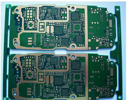
What are the principles to be followed in the process of PCB copying?
PCB copying is a very tedious task. If you are not careful, mistakes will be copied and the circuit board can no longer be used. So, what are the principles to be followed in the process of PCB copying?
1. Wire width selection: 40-100MIL wire width can meet general application requirements. For high-power applications, the wire width should be appropriately increased according to the power. In low-power digital circuits, in order to increase the wiring density, the minimum line width is 10-15MIL.
2. Line spacing: When the line spacing is 1.5MM (about 60MIL), the insulation resistance between lines is greater than 20M ohms, and the maximum withstand voltage between lines can reach 300V; when the line spacing is 1MM (40MIL), the maximum withstand voltage between lines It is 200V. Therefore, on medium and low voltage (line-to-line voltage not greater than 200V) circuit boards, the line spacing is 1.0-1.5MM (40-60MIL).
3. Pad: For a 1/8W resistor, a diameter of 28MIL is sufficient; for a 1/2W resistor, the diameter is 32MIL.

4. Draw the circuit frame: the shortest distance between the frame line and the component pin pad should not be less than 2mm, generally 5mm is more reasonable, otherwise it will be difficult to blank the material.
5. Component layout principle: In PCB design, if the circuit system has both digital circuits and analog circuits, as well as high-current circuits, they must be laid out separately to minimize the coupling between the systems in the same type of circuit.
6. The input signal processing unit and output signal drive components should be close to the side of the circuit board, and the input and output signal lines should be as short as possible to reduce the interference of input and output.
7. Component placement: It can only be arranged in two directions, horizontal and vertical.
8. Component spacing: For medium-density boards, the component spacing can be 50-100MIL during wave soldering; for integrated circuit chips, the component spacing is generally 100-150MIL.
9. When the potential difference between components is large, the spacing should be large enough.
10. The IC decoupling capacitor should be close to the power supply pin of the chip, otherwise the filtering effect will be worse.
11. The clock circuit components are as close as possible to the clock signal pins of the microcontroller chip to reduce the wiring length of the clock circuit.
The above are some of the principles to be followed in the process of PCB copying. How much do you have? ipcb is a high-precision, high-quality PCB manufacturer, such as: isola 370hr PCB, high-frequency PCB, high-speed PCB, ic substrate, ic test board, impedance PCB, HDI PCB, Rigid-Flex PCB, buried blind PCB, advanced PCB, microwave PCB, telfon PCB and other ipcb are good at PCB manufacturing.