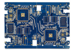
One of the basic functions of PCB is to carry the transmission of electrical signals.
To study the reliability of PCB is to study whether its basic functions are not lost or some of its electrical performance indicators are not deteriorating, that is, the durability of its functions. This paper intends to study the reliability of PCB from three aspects: the quality of downstream PCB users after installation, the quality of direct user debugging and the quality of product usage, so as to characterize the quality of PCB processing and provide the basic way to produce high reliability PCB.
Reliability Analysis of 1 PCB
Quality Characterization of 1.1 PCB after Installation
After PCB installation, the quality of PCB is directly reflected in:
Visually check the appearance of PCB whether there are frothing, white spots, warping and other phenomena.
One of the concerns is that bubbling, which is called "explosion board or stratification" by industry insiders, should not occur after the installation of a reliable PCB. In order to obtain high reliability PCB, the following aspects must be started.
Selection of 1.1.1 PCB Material
The performance of the same type of PCB base material differs greatly from different manufacturers, and the performance of different types of PCB base material differs even more. PCB processing chooses the base material to take into account both the heat resistance of the material and the electrical performance of the material. In terms of installation, we consider the heat resistance of the material more. The thermal resistance of materials is generally referred to as glass transition temperature (Tg) and thermal decomposition temperature (Td). At present, the PCB installation is divided into lead, lead-free and mixed installation according to the solder joint composition (lead and lead-free) of the components. The corresponding peak reflow soldering temperatures are 215, 250 and 225 degrees C. Therefore, PCB materials should be selected differently for different installation methods. For lead-free soldering, plates with Tg higher than 170 C are selected. For mixed-assembly welding, plates with Tg higher than 150 C are selected.
For lead soldering, all materials are suitable, but Tg plates higher than 130 C are usually used. In addition to considering Tg, general attention should be paid to the manufacturer's brand and model. At present, the commonly used plates with stable performance are Tuc, IsoIa, Hitachi, Neleo, etc.
1.1.2 Process Control
Before PCB leaves the factory, samples should be taken to conduct the delivery state and thermal stress test, the purpose of which is to ensure that the installation is not stratified, etc. Although the product with defective delivery state and fully qualified thermal stress test cannot be guaranteed to be installed without defects, there must be hidden dangers when the product with defective delivery state is installed. Therefore, the delivery state and thermal stress test are early predictors of installation quality. In this way, delivery status and thermal stress qualification are necessary for PCB delivery. For this reason, attention should be paid to the following aspects during the processing of PCB to ensure that the delivery state and thermal stress test are qualified and to improve the quality after installation.
1.1.2.1 Define PCB processing requirements
The PCB thermal stress test results are influenced by the number of layers, thickness, BGA pitch (or center distance between holes), Conductor Copper thickness, etc. Plates with more than 12 layers and thicker than 3.0 mm are prone to micro-cracks and hole wall defects after thermal stress due to the large Z-axis expansion and contraction value.
The BGA pitch is less than 0.8 mm or the hole wall center distance is less than 0.5 mm. Due to the large heat capacity, the heat is concentrated during installation, which easily causes the dielectric layer to be stratified. Therefore, materials with Tg higher than 170 C should be selected for processing such PCB.
Conductor thickness greater than 35 μ M, high heat capacity, high resistance to resin flow, use as many high fluidity semi-cured sheets as possible during lamination. For PCB with a hole diameter less than 0.3 mm, the quality of drilling directly affects the quality of the hole wall. The drilling parameters should be strictly controlled to ensure that the hole wall is clean, flat and tear small.
1.1.2.2 Fine Process Control
Layering occurs in the alternating state and thermal stress experiments. The main reason is that the defect of oxidation treatment quality of inner conductor results in poor adhesion of copper to semi-cured sheet or the staining or moisture absorption of semi-cured sheet. The oxidation process varies depending on the material. High Tg materials are hard and brittle, and are oxidized by velvety brown. Conventional materials may be oxidized by crystalline black [2]. Of course, the roughness of conductor surface directly affects the binding force of copper to semi-cured sheets. Therefore, no matter what kind of oxidation treatment, the surface roughness of oxidation must be clearly defined. At the same time, during the lamination process, the contamination and moisture absorption of materials should be avoided as much as possible. For this reason, the baking conditions of the single sheet must be controlled quantitatively, the semi-cured sheet must be dehumidified, and the cleanliness of the environment and the operating specifications must be controlled in the laminate. In the control of the lamination process, effective lamination parameters must be established according to the type and quantity of the plates to ensure adequate wetting of the resin and flow rate to avoid voids.

Characterization of debugging quality of 1.2 PCB
The quality of PCB debugging mainly depends on whether the debugging result satisfies the design requirements smoothly. After installation, the PCB debugging smoothly involves the processing quality of PCB, which is also an important information to characterize the reliability of PCB. Generally, the board with smooth debugging has high reliability. On the contrary, if the board is not debugged smoothly, there must be hidden dangers in its reliability. The processing quality of PCB mainly involves the line, disc and media layers of PCB.
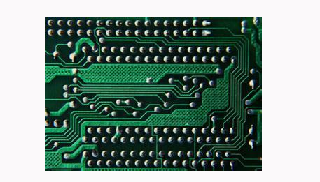
Effect of 1.2.1 PCB conductor on PCB quality
With the fine development of electronic products, along with the continuous improvement of PCB processing technology, PCB wires are no longer simple signal transmission, but supplemented by many functional requirements such as impedance lines, contour lines, reactance lines and so on. As a result, defects of wires such as gaps, burrs, shape corners etc. have more and more obvious influence on the performance of PCB (3). 10% deviation of line width may cause impedance changes of up to 20%. Gaps and burrs of wires can delay the signal up to 0.1 ns. Shape differences of wires can cause reflection, noise and other interference to affect the integrity of signal transmission. It can be seen that the quality of the line can not be ignored in the process of making printed board. On the one hand, strict process control is required, on the other hand, high-precision production equipment and appropriate process technology (such as semi-addition and addition) are required to ensure that the accuracy of the line meets the design requirements.
Effect of 1.2.2 PCB Connecting Disk on PCB Quality
Connecting disc usually has a large aperture. The ring width requirement is taken into account in the design. The quality can be guaranteed, but the quality of the holes varies greatly from manufacturer to manufacturer. With an aperture larger than 0.6 mm and a window-opening coating of Pb/Sn, it is unlikely that the problem will occur. However, for holes smaller than 0.3 mm, different roughness, different depth of tearing, different thickness and uniformity of holes wall are caused by different parameters of small holes and bad solution exchange. As far as possible, different through-hole coating processes, such as covering with solder-resistant ink or even blocking holes, will be adopted in the future, but blocking holes have little effect on the resistance of holes. Therefore, the difference in pore resistance still exists. Table 1 lists the resistance test results of 0.25 mm holes from different manufacturers.
Table 1 Hole Resistance Difference
Table 1 Hole Resistance Difference
The large pore resistance affects the quality of electrical signal transmission, at the same time, it also refracts the existence of non-conductive impurities or holes or cracks in the pore wall. Such holes, impacted by high temperatures, will inevitably produce cracks or cracks, resulting in complete loss of function to form PCB. Therefore, in the processing of PCB, special attention must be paid to the size of the hole resistance value.
Effect of 1.2.3 PCB Layer on PCB Quality
The layer of PCB refers to the thickness and uniformity of the processing material and the interlayer dielectric layer of PCB, which has been described before, with emphasis on the thickness and uniformity of the dielectric layer.
The thickness of dielectric layer affects the interlayer insulation of PCB, and its characteristic parameter is breakdown voltage. The higher the breakdown voltage, the better the insulation. The breakdown voltage of PCBs used in different fields may be different, but the dielectric layer is thin, the breakdown voltage must be low, and the dielectric layer with the same thickness is thicker, so the control of dielectric layer thickness is based on the breakdown voltage and gives consideration to the type of semi-cured sheets. The uniformity of dielectric layer thickness affects the stability of signal transmission. The thickness deviation is 10%, and the characteristic impedance deviation can be up to 20%. Thickness uniformity, on the one hand, is related to material performance parameters such as gel time, resin fluidity, etc. On the other hand, it is closely related to the process parameters of lamination and the accuracy of the equipment. Therefore, the uniformity control of dielectric layer thickness needs to be controlled by high precision equipment and optimized lamination parameters.
Characterization of 1.3 PCB Usage Quality
The stability of performance in the use of electronic products is related to the quality of PCB. The defects of PCB commonly encountered in use are ion migration (CAF) and solder quality (Joint). Copper ion migration system results in copper migration between two conductors such as pore wall to pore wall through the slit between glass fibre bundle or yarn bundle and resin. The mechanism is that after PCB is powered on, copper at high voltage (anode) first corrodes in water and then oxidizes to copper Cu2+. Copper ions migrate slowly along the channel to the other low voltage pole. The low voltage end also moves to the anode, so that copper can be restored from the two when they encounter the channel on the way, forming a connection between the two places, that is, a leakage short circuit. Once a short circuit occurs, the CAF will be burned by high resistance heat, and then a new CAF will be started. This happens week after week, sometimes without the functionality of electronic products. Here are several scenarios where CAF occurs.
It can be seen that the CAF must be produced under the following five conditions: bare copper conductor, water vapor, electrolyte, potential difference and channel. The first four items are unavoidable in the use of electronic products. Channels can be used to control the generation of CAF, and the formation of channels is mainly related to the material, drilling, contamination and other factors in the production of PCB. Generally speaking, the finer the glass fibre, the higher the resin content, the better the toughness and the lower the probability of drilling tear. Therefore, as far as possible, the fine glass fibre material should be used for PCBs used in high density PCC or humid environment. Different material, different number of holes, different drilling parameters, when drilling, the impact of the drill on the reinforcement material is different, the quality of the hole wall is different, the damage to the hole wall is also different, and the core suction degree is different. Therefore, in order to prevent the occurrence of passage, the quality of drilling holes should be strictly controlled to ensure smooth and flat hole walls. The main purpose of contamination removal is to remove the resin adsorbed when drilling holes in the inner conductor. Of course, the resin in the insulation layer of the hole wall is also bitten. Sometimes, in order to form negative etching, the resin in the insulation layer of the hole wall even bites more. At this time, the amount of bite should be strictly controlled. Otherwise, it is very easy to form a "channel".
The picture below shows resin bite excess.
PCB and components are connected by welded solder joints, which sometimes occur abnormal conditions due to environmental impact in the use of electronic products. This is mainly related to the surface coating process of PCB. At present, PCB surface is coated with hot air leveling, tin plating, chemical nickel-gold, organic anti-oxidation protection, silver and so on. Cu6Sn5IMC formed during hot air leveling or tin-plated welding will not change in long-term use. The solder joints are firm and reliable. Due to the uneven wiring of chemical nickel-gold, it is unavoidable to produce "nickel oxide" black pad. At the same time, Ni3Sn4 IMC is formed during the welding process, with the infiltration of gold and phosphorus, the solder joints are fragile and the reliability decreases during long-term use. The OSP bonds form Cu6Sn5 IMC, and there is no contamination from other metals (such as Au, Ag). They have good strength and reliability. Silver-impregnated solder joints form Cu6SnIMC, which has good strength but is not resistant to aging. Silver-impregnated solder joints may form micro-voids. Cu6Sn5 is formed at the edge of the tin dipped solder joint, but the tin dipped layer is gradually absorbed by the bottom copper and becomes IMC. The appearance changes from bright white to gray white. In electroplating Ni-Au, the quality of solder joints is gradually affected by the penetration of gold, although there is less phosphorus and black pad to dry up and the strength of solder joints is high. Therefore, the choice of coating on PCB surface affects the quality of solder joints and involves the use effect of electronic products. Therefore, in high reliability product design, PCB surface coating is preferred for hot air leveling or OSP.
2 Conclusion
(1) The reliability of PCB can be characterized from three aspects: post-installation quality, debugging quality and use quality. (2) Installation quality involves material selection and process control. (3) Debugging quality is closely related to the accuracy control of PCB basic elements; (4) The quality of use is related to the environment and the choice of surface coating.