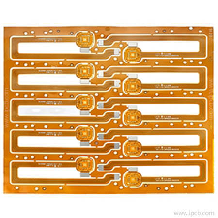
The demand for data transmission speed and smaller size of modern electronic equipment is increasing day by day, and the development of flexible circuit boards is continuously promoted. A rigid-flex printed circuit board (PCB) is composed of a rigid motherboard and a flexible circuit. The flexible circuits on some layers are directly connected to the rigid motherboard (Figure 1). Rigid-flex board has smaller volume, lighter weight and lower cost, and is widely used in modern electronic equipment. Excellent curvature, suitable for small spaces and low manufacturing costs, these characteristics make it an ideal choice for mobile communication products.
Electromagnetic (EM) analysis of rigid-flex PCBs has always been difficult, and it is necessary to model the complex process of bending and mounting the circuit board into a small space. The workflow based on the Cadence® Clarity™ 3D Solver field solver provides the necessary tool interoperability to help designers use 3D finite element analysis (FEM) to accurately verify the signal integrity of rigid-flexible wires. Compared with the traditional process that relies on manual design, this workflow can efficiently set up the EM simulation environment and reduce errors.
Cadence Allegro® PCB Editor can help designers easily create and visualize circuit boards, and is widely used in rigid-flex PCB design. The specific functions of this tool include rigid-flexible deformation (such as bending), multiple flexible composites that support flexible circuit coverage, rigid-flexible partition management, and coverage and gap inspection (such as interlayer inspection). After the PCB designer's reference guide installs the components in a specific space and completes the circuit board layout (ECAD), the ECAD data will be imported into the Clarity 3D Solver for complete 3D FEM EM simulation. Clarity 3D Solver is used in the key interconnection design of PCB, IC packaging and system-on-chip (SoIC). It adopts Cadence distributed multi-processing technology to provide nearly unlimited processing power and 10 times faster speed for large-scale designs.
Compared with the simulation of plane PCB geometry configuration, the rigid-flex PCB needs to combine the rigid circuit board with the 3D flexible board that can be bent and twisted in any direction (Figure 2), and the workflow is more complicated. The traditional design method of rigid-flex board uses the mechanical computer-aided design (MCAD) process. The circuit board is first imported into 3D MCAD tools such as AutoCAD for 3D bending, and then the bent circuit board is a .step/.iges/.sat The file format is exported to the 3D EM tool for S-parameter extraction. This process often causes human error due to the mismatch of the through hole and the layer and the length mismatch during bending. Problems are unavoidable when the EM tool is defined in material properties and port creation. . Even if the entire process is successfully completed, EM simulation may not be possible due to design complexity and meshing issues. Designers will be forced to fall into a vicious circle of simulation settings from MCAD tools, to geometric configuration remodeling, and to EM engine. This iterative process requires cumbersome user communication and is extremely time-consuming, depending on the scope of the design, from a few hours to a few days, or even a few weeks.

Automated workflow
The Cadence workflow adopts a fully automated and easy-to-use solution, which well meets the challenge of rigid-flexible bending analysis. The designer can easily complete the setup in just a few minutes. The process is divided into 5 steps:
1. Define the parameters in Allegro PCB Editor software.
2. Import the defined parameters into the Clarity 3D Solver environment, and verify the accuracy of the stacked physical properties, networks, components, and different areas.
3. Use the automated port tool to define the port.
4. Import the obtained .spd file into the Clarity 3D Solver workbench environment.
5. Define the frequency and frequency sweep of the solution and start the simulation.
To further describe the details of the automated workflow, we used the Clarity 3D Solver of 10 GHz and set the frequency sweep from 10 MHz to 10 GHz to simulate a rigid-flex PCB with three bends. Clarity 3D Solver's automatic adaptive finite element mesh encryption function can maintain the accuracy of rigid-flex PCB. Parallelization technology ensures that grid division and frequency scanning can be partitioned and distributed on multiple computers, reducing the overall time for simulating complex rigid-flexible structures. Figure 4 shows the simulation |S21| and |S11| of the selected grid of the rigid-flex board. Figure 5 describes the meshing and the surface current density of the metal layer, and the modeling method of flexible PCB bending.
The rigid-flexible PCB workflow shows the acceleration of the product design cycle by integrated design and EM analysis solutions. This simple and efficient workflow for rigid-flex PCB EM analysis can save PCB and EM designers a lot of design and analysis time. EM engineers can use the Clarity 3D Solver in this workflow to PCB simplify design steps, quickly develop products, and shorten time to market.