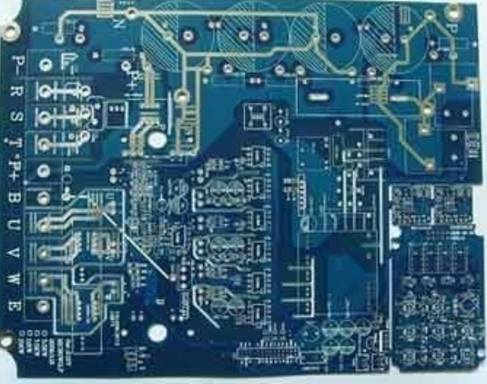
Copper coating is an important part of PCB design. Both domestic Qingyuefeng PCB design software and some foreign Protel and Power PCB provide intelligent copper coating function. So how to apply copper well, I will share some of my ideas with you, hoping to bring benefits to peers.
The so-called copper coating is to take the idle space on the PCB as a reference level, and then fill with solid copper, these copper areas are also called copper filling. The significance of copper coating lies in reducing grounding impedance and improving anti-interference ability. Reduce voltage drop, improve power efficiency; Connecting to the ground also reduces the loop area. For the purpose of keeping PCB welding from deformation as much as possible, most PCB manufacturers also require PCB designers to fill copper skin or grid-like ground wire in the open area of PCB. If copper coating is not properly handled, it will not be rewarded and lost. Is copper coating "more beneficial" or "more harmful"?

It is well known that at high frequencies, the distributed capacitance of the wiring on the printed circuit boards come into play. When the length is greater than 1/20 of the corresponding wavelength of the noise frequency, an antenna effect will occur, and the noise will be emitted through the wiring In the existence of bad grounding coppercoating, copper coating became a tool to spread noise, therefore, in the high-frequency circuit, do not think that the ground somewhere connected with the ground, this is the "ground", must be less than λ/20 spacing, in the wiring hole, and the floor of the multilayer board "good grounding". If the copper coating is properly treated, the copper coating not only increases the current, but also plays a dual role of shielding interference.
Copper coating generally has two basic ways, is a large area of copper coating and grid copper, often someone asked, a large area of copper coating or grid copper coating is good, not generalize. Why is that? Large area copper coating, with increased current and shielding dual role, but large area copper coating, if the wave soldering, the board may become up, and even bubble. Therefore, a large area of copper coating, generally will open a few slots, alleviate copper foil foaming, pure grid copper coating is mainly shielding, increase the role of current is reduced, from the perspective of heat dissipation, grid has the advantage (it reduces the heating surface of copper) and has a certain role in electromagnetic shielding. But it should be pointed out that, the grid is made by alternating direction of running, we know for circuit line width for the work frequency of the circuit board has its corresponding "electricity" length of (actual size divided by the work frequency of the corresponding digital frequency, concrete books), when the working frequency is not high, perhaps the role of the grid lines is not obvious Once the length of the electricity matches the operating frequency, it gets really bad. You find that the circuit doesn't work at all and there are signals going off all over the place that interfere with the system. So for those who use grid, my advice is to choose according to the design of the circuit board, do not cling to one thing. So the high-frequency circuit against interference requirements of high multi-purpose grid, low-frequency circuit has a large current circuit and other commonly used complete copper laying.
Having said so much, we need to pay attention to those problems in copper dressing in order to achieve the desired effect of copper dressing:
1. If PCB ground is more, there are SGND, AGND, GND, etc., it is necessary to use the most important "ground" as reference to coat copper independently according to the different PCB board position. Digital ground and analog ground are used separately for copper coating. At the same time, before covering copper, first thicken the corresponding power line :5.0V, 3.3V, etc., so that Multiple deformation structures of different shapes are formed.
2. For different points of the single connection, the way is through 0 ohms resistance or magnetic beads or inductance connection;
3. Copper coating near the crystal oscillator, the crystal oscillator in the circuit is a high frequency emission source, the approach is to surround the crystal oscillator copper coating, and then the crystal oscillator shell separately grounded.
4. Island (dead zone) problem, if feel big, then define a hole to add it is not much trouble.
5. At the beginning of the wiring, the ground should be treated equally, when the wire should walk the ground, can not rely on copper coating by adding holes to eliminate the connection of the pin, this effect is very bad.
6. It is better not to have sharp angles on the board (" =180 degrees "), because from the point of view of electromagnetism, this constitutes a transmitting antenna!
7. The wiring of the middle layer of multilayer board is open area, do not apply copper. Because it's very hard to make this copper pack "well grounded."
8. The metals inside the device, such as the metal heat sink and metal reinforcement strip, must be well grounded.
9. The heat dissipation metal block of the three-terminal regulator must be well grounded. The grounding isolation belt near the crystal oscillator must be well grounded. In short: the copper coating on PCB, if the grounding problem is well dealt with, it is certainly "more good than bad", it can reduce the backflow area of the signal line, reduce the signal external electromagnetic interference.